In addition to the design rules, there are three major considerations that must be accounted for. The most important of these is the order of the series devices of any logic gate.
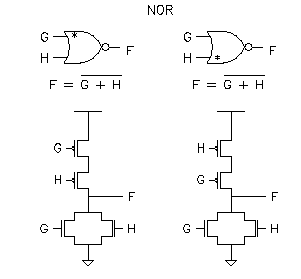
When drawing the layout for devices under 30 MHz, the order of the series devices normally don't matter. However, modern microprocessors have speeds that exceed 300 MHz. Under these circumstances, even a couple nanoseconds of delay could cause signals to no longer be timed correctly. Because of this, additional symbols can be added to the schematic symbol to represent the relative order of series transistors. In this series of pages, the asterisk will represent "top of the stack." The "stack" is the term used to describe any series path.
In this case, G is "top of the stack" (top of the series circuit). Another layout consideration is designed to prevent the problem seen in the last section.
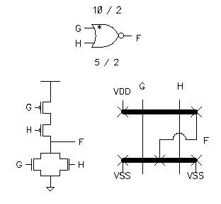
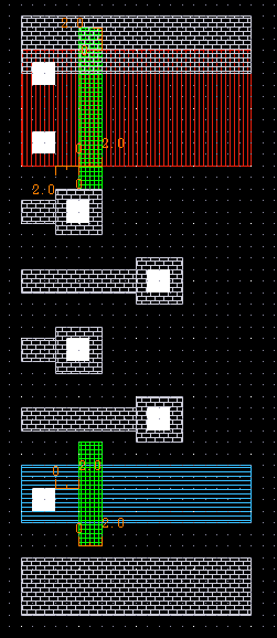
When dealing with multiple metal inputs, there needs to be enough room between the devices to accommodate the required number of metal lines. If there was room reserved for metal lines between the N-FETs and P-FETs, the need to go back and expand the height of the drawn layout would be greatly reduced.
This template has room for 4 metal lines in the middle. The N-type diffusion can expand down, while the P-type diffusion can expand up. The metal VSS and VDD power bus is also placed in this template. A two-input NOR gate can be drawn using this template.
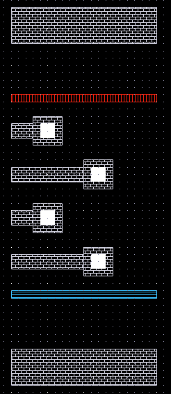
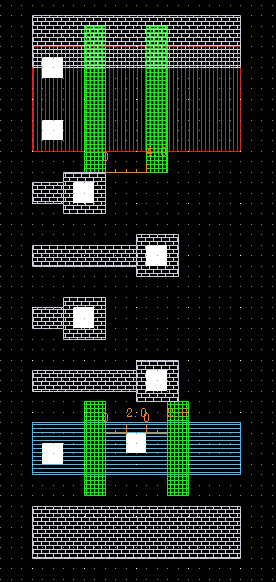
Since the N-type and P-type diffusion are already spaced out, both the N-FETs and P-FETs can be created at the same time. Once the right most contacts are placed down, the first polysilicon can be placed.
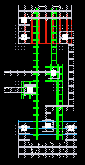
Now the second polysilicon can be placed. Remember that for the N-FETs there are contacts between the gates, but for the P-FETs there are no contacts.
The last set of contacts now need to be placed, as well as the metal enclosure of contacts and the interconnect.
Since not all of the reserved metal1 lines were needed, the ones not used should be deleted. The last major consideration is tying the die to VSS and the N-Well to VDD. If the substrates are not tied to VSS and VDD, an event called latch-up can occur. Latch-up creates a short between VSS and VDD through the die and N-Well. Ties are made of the same type of material as the substrate. N-Well ties are made of N-type diffusion, and P-type ties are used outside of the well.
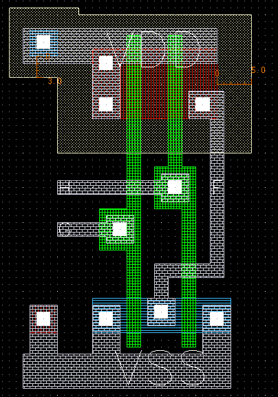
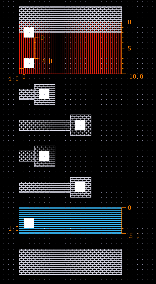
According to the design rules, opposite type diffusions must be 5 microns away from each other. This is the layout of a two-input NOR gate, with taps drawn. Taps are required for every layout.