= HF8V = / = SP8WJT = / = SP0106RZ =
HF-17266
PROJECT: HF-17266
DESCRIPTION: Fiscal Printer DF302 LB130FM6 POSNET
TYPE: DF302, LB130FM6
BRAND: POSNET
STATUS: q
PROJECT START DATE: 2018
LOCALISATION: PL
DOCUMENTATION: TM (7 pages, PCB drawings, circuit diagram, GAL functions tables)
PCB: TPD58266
DIMENSIONS: 130 x 84 mm
HARDWARE VERSION: 2.03
SOFTWARE VERSION: 0.00
CPU CATALOG NUMBER: UC-291
CPU: SC87C51
CPU BRAND: INTEL (SIGNETICS)
FAMILY: '51
ROM: 4 KB
RAM: 128
ADR SPC: 64 KB
MAX CLOCK: 12 MHz
THN ADDRESS: 0x37
TYPE: 0x28
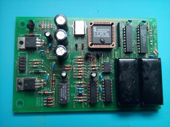
HF-17266 version 2.01
It was polish production fiscal printer main board. I cutted original TPD57266 to TPD58266 removing some glue electronics, not particullary needed for me and in this way obtaining more compact system. Originally processor works on internal memory but it is not problem to switch it on external memory.
Complete reverse engineering has been made, I recreated circuit diagram, PCB assembly drawings, rescanned and tested functions of GAL chip, so now is time for software part. It will be more probably my THOS operating system.
PLCC44 socket allows me testing several other '51 CPUs in my collection.
U1: SC87C51 - CPU - PLCC44 removable
U2: 74374 - LATCH - address/data multiplexing
U3: 27C512 - ROM0 - MM-431
U4: 27C512 - ROM1 - MM-432
U5: 74LS07 - desoldered
U6: 7414 - 6 x INV
U7: GAL16V8 - PAL - memory mapping, reset
U8: 4020 - counter
U9: LM555 - desoldered
U10: 7805 - REGULATOR 5V (for memories)
U11: 7805 - REGULATOR 5V (for system)
U12: 74HCT08 - 4 x 2AND
U13: 24C02 - EEPROM - MM-433
| Original circuit description |
In original circuit CPU worked from internal memory (4 KB) where some kind of operating system was present, with additional data stored in two 27C512 chips (2 x 64 KB). Data looks like printer calibration 32 byte records and NIP identifier.
GAL chip is used for memory mapping and also some kind of hardware generator was present (LM555, 4020, GAL). That generator is still unclear for me because I removed that PCB part before analyzing circuit. It can be something with other hardware connected, or maybe some kind of voltage supervisor for resetting CPU.
Other glue electronic is used as UART buffers (U12) because 87C51 has weak ports, EEPROM is present, there is some kind of voltage comparator for testing supply voltage, etc...
Two separate 7805 regulators were used, one for system and another for memories only. Maybe they had problems with voltage stability, what is possible when power supply is bad quality, often high current printer motors are present in such systems.
There was no RAM chip on board, interesting why, maybe it was a kind of terminal system without graphics, so in my modifications I will replace one of ROMs with RAM.
More circuit details can be found in my paper Project Files: [2] - [9]. I have no time to create electronic version (and I like paper version more), but it can be helpfull for you if you have the same module and you want to modify this or repair.
1/ Inital tests, cleaning, recreating circuit diagram (version 1.00)
2/ Removed U5, U9 (version 2.00)
3/ Part of PCB cutted off, reregistered to TPD58266 (version 2.01)
4/ CPU PLCC44 socket desoldered and some connections modified. EA/ input moved from VCC to GND (switched to external memory) (version 2.02)
5/ Desoldered ROM0, ROM1 for memory downloads. Memories MM-431 and MM-432 dowloaded. (version 2.03)
6/ Modifications DIP28 memory circuit to DIP32 memory circuit (includes rerouting some paths from CPU and PAL) (version 2.04)
7/ 32KB RAM memory mounted in place of ROM1 and DIP32 FLASH in place of ROM0 (version 2.05)
8/ Replacing 24C02 with 24C08 (version 2.06)
See HARDWARE VERSION for current state.
[1] SC87C51 datasheet
[2] HF-17266 TM front page
[3] HF-17266 TM page 1 - project info
[4] HF-17266 TM page 2 - index page
[5] HF-17266 TM page 3 - assembly drawings
[6] HF-17266 TM page 5 - circuit diagram
[7] HF-17266 TM page 6 - ICs, configuration description
[8] HF-17266 TM page 7 - PAL transfer functions
[9] HF-17266 TM page 8 - PAL transfer functions
[10] no$x51 - very nice DOS retro simulator, disassembler and assembler for MCS-51
Prefix 17
HF Register
Microcontrollers in my constructions
UC Database - my CPU collection
Electronics
Main Page
Generated by HF Projects Page Creator ver. 2.03