Objectives: At the end of this chapter the student will be able to:
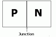
Discrete semiconductor device is made of one or more PN junctions, thus, the study of PN junction is very important in order to understand its basic operation. When half of a pure single crystalline semiconductor material is doped with trivalent element and the other half with a pentavalent one, a PN junction is formed. A PN junction is a boundary or a joint of P- and N- type semiconductor crystal. Figure 1.1 is a simplified construction of a PN junction.
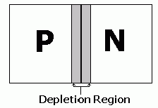
During the period of transition or contact of P-type and N- type semiconductors, a natural phenomenon occurs instantly. Majority current carriers, holes and free electrons, diffuse in either side to recombine in the junction only in a very short period of time. Recombination is the process where free electrons and holes unite and vanish. The occurrence of this phenomenon resulted in the creation of a space charge or depletion region. This is the region near the junction where majority current carriers are greatly diminished or depleted. During recombination atoms near the junction are ionized. Atoms in the P-type region near the junction gain electrons. They become a negatively charge ions. Atoms in the N-type region near the junction lost electrons, they become a positively charge ions. It takes only a short time for the charges of both ions near the junction enough to repel majority current carriers that will recombine further in the junction. The pair of positive and negative ions is called dipoles; they remain uncompensated in the region near the junction. This region is a charge space or depletion region and is depleted with majority current carriers.
Figure 1.2 shows the depletion region in a PN junction.
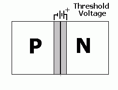
Due to non-uniform distribution of dipoles in the depletion region, an electric field and potential difference exist in the junction. Threshold voltage is the static-potential difference variation with the polarity same as the polarity of ionized atoms near the junction. The net charge of the material is zero since the number of minority current carriers attracted by these dipoles, the drift saturation current, are equal to the small number of majority current carriers that leaves the particular regions that recombined in the junction through diffusion, hence equilibrium is achieved. The threshold voltage is equal to 0.7 volt for Si, 0.3 volt for Ge and 1.2 volts for GaAs made PN junctions. Figure 1.3 shows the polarity of threshold voltage in a PN junction.
This potential barrier is the reason why there is only a minimal recombination of majority current carriers in the junction this is through diffusion. In order for them to recombine in the junction in maximum as a drift current, an applied potential equal to the magnitude of threshold voltage in opposite direction is to be employed.
Figure 1.4 shows an applied voltage or bias to offset the effect of threshold voltage.
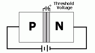
Figure 1.4 is an illustration of a forward biased PN junction. The applied voltage pushes both free electrons from the N-type region and holes from the P-type region towards the junction for recombination for a current to flow in the circuit. In this case the depletion region is reduced to a minimum level. The resistances offered by the material to this drift current are only the bulk resistance and the junction resistance. Ideally the resistance of a forward-biased PN junction is zero. The bulk resistance is the resistance of the body of the material and the junction resistance is equal to 0.026 volt divided by the amount of dc current that flows in the device at room temperature.
The voltage drop across a forward-biased PN junction is nearly equal to the threshold voltage. The following must be true for a forward biased PN junction:
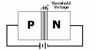
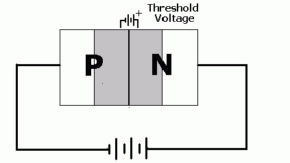
Figure 1.6 illustrates a reverse biased PN junction. Note the polarity of the applied voltage with respect to both P-type and N-type materials. Due to this, the holes in the P-type region is attracted away from the junction by the negative side of the applied voltage, and the free electrons in the N-type region is also attracted away from the junction by the positive side of the applied voltage. This resulted to the widening of the space charge or depletion region.
The majority current carriers flow in the device is zero. A small or negligible amount of minority current carriers flow is present in the device due to recombination in the junction and this is known as the leakage current. The amount of leakage current is maintained to a negligible level until such a condition exists for breakdown to occur. This will lead to rapid increase of magnitude of leakage current. This exponential increase of leakage current if not contained will bring the device to its destruction.
The following are true for a reverse biased PN junction:
The depletion region acts as an insulator that separates the P- and N-type materials of the PN junction. The PN junction seems like a capacitor with the depletion region as the dielectric that separates the two polarized plates, the P- and N- type regions. The capacitances offered by the PN junction during its forward and reverse bias states are called junction capacitances. The effect of these capacitances is considered if the PN junction is exposed to high frequency applications.
The time to switch the forward-biased PN junction to fully reverse-biased one is called reverse recovery time or junction switching time. This is due to the short period of current flow after the applied voltage has reduced to zero and clearing of majority current carriers from the region near the junction.
When the applied voltage is equal to the voltage breakdown of the junction, the leakage current increases exponentially and if not contained will destruct the device. There are two principal mechanisms of breakdown, the field emission and ionization by collision. Field emission is the tearing off of valence electron from its valence shell to become free electron due to the presence of strong electric field in the junction. This is known as the Zener effect. Zener effect happens less than 4 volts of the applied voltage.
Ionization by collision is due to the collision of free electron and the valence electron. A high velocity free electron can dislodge a valence electron from its valence shell to become another free electron. This has a multiplicative effect thereby increasing the magnitude of the leakage current. This is known as the avalanche effect. The avalanche effect happens with applied voltage at least 6 volts.
The following are the only few semiconductor devices that are made of PN Junctions:
Draw the basic construction and schematic symbol of the semiconductor listed in topic outline III. List other 10 semiconductor devices and draw also their basic construction and schematic symbol. Do this in separate sheets of paper. Return to Top