|
|
|
|
|
|
|
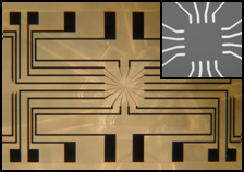
In my PhD research, we
used directed assembly methods to grow nanowires between targeted points in external circuitry. We performed transport measurements
on
as grown nanowires without any post-growth processes which are required
to interface nanowires with external circuitry in other approaches. We
also did detailed structural characterization on these nanowires. |
|
|
Initially, we formed interconnects dielectrophoretically
from gold nanoparticles. We were able to form wires from cadmium
sulfide (CdS) nanoparticles. These wires formed very fast which
can be seen in this CdS wire formation
movie. We also observed
bursts of luminescence from CdS wires as we continued to
apply voltage after the formation of the wire. |
|
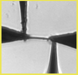
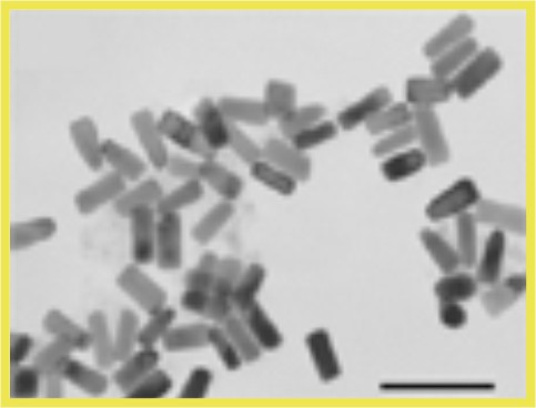
We employed dielectrophoresis to form wires from gold nanorods (right image). We observed
Coulomb Blockade to charge conduction in these wires due to their
nanoparticulate structure. |
|
|
|
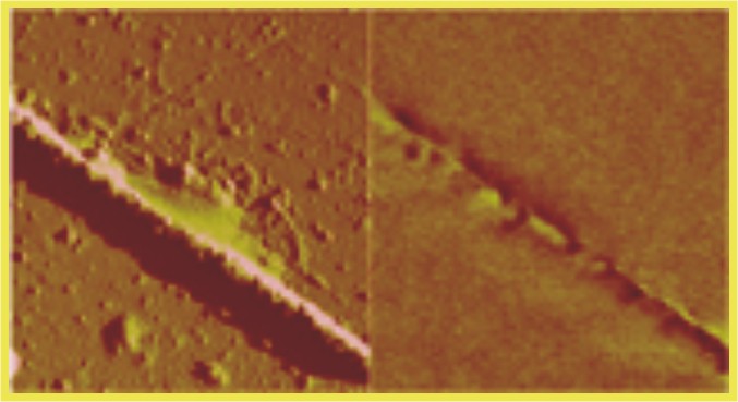
Recently, we developed a
new technique that we call Directed Electrochemical
Nanowire Assembly (DENA). This technique enables the growth of crystalline, metallic
nanowires between targeted points in the external
circuitry from simple salt solutions of the desired metals. |
|
|
|
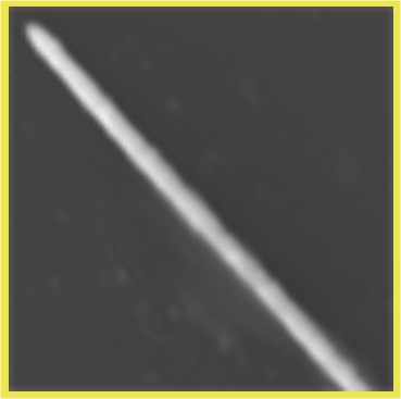
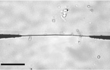
We were able to form
single-crystal indium wires from indium acetate solution (left image)
using DENA technique. You can watch a movie of the crystalline indium
wire growth by clicking on the left image.
|
|
|
We
also demonstrated the DENA growth of near-single crystalline gold
nanowires and their low-contact resistance interfacing with lithographic
electrodes. We extended metallic
wire formation from simple salt solutions to other metals such as lead,
zinc, silver, copper,
cobalt and nickel.
|
|
|
|
|
|