1. Physical Layer
The Physical Layer processes outbound packets before transmission to the Link and processes inbound packets received from the Link. The two sections of the Physical Layer associated with transmission and reception of packets are referred to as the transmit logic and the receive logic
1.1 Sub-blocks in Physical Layer
Two sub-blocks make up the Physical Layer. They are
• Logical Physical Layer
• Electrical Physical Layer
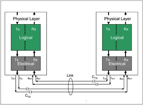
Fig: 1 Logical and Electrical Sub-Blocks of the Physical Layer
Both these sub-blocks are split into transmit logic and receive logic (independent of each other) which allow dual simplex communication.
1.2 Transmit Logic
The transmit logic of the Physical Layer essentially processes packets arriving from the Data Link Layer, then converts them into a serial bit stream. The bit stream is clocked out at 2.5 Gbits/s/Lane onto the Link.
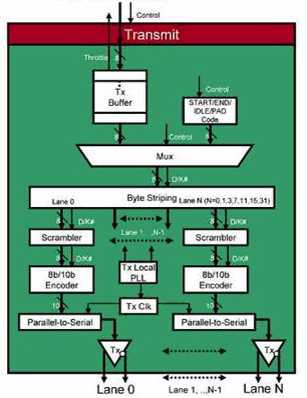
Fig: 2 Physical Layer Transmit Logic Details
1.2.1 Elements that make up the transmit logic :
• Transmit Buffer (Tx-Buff),
• A multiplexer (mux),
• Byte striping logic (only necessary if the link implements more than one data lane),
• Scramblers,
• 8b/10b encoders,
• Parallel-to-serial converters.
1.2.1.1 Transmit Buffer (Tx-Buff)
The Tx Buffer receives TLPs and DLLPs from the Data Link Layer. Along with the packets, the Data Link Layer indicates the start and end of the packet using a 'Control' signal so that the Physical Layer can append Start and End framing characters to the packet.
1.2.1.1.1 Implemented Specifications
• The width of Tx-buffer is 8-bit and height is 22.
• Receives TLP or DLP from the buffer in DLL. The packets are received through 8-bit bus. The transfer process is synchronized with internal clock.
• Sends data to Multiplexer only when Control signal is 1 (i.e. #D)
• Sets Packet_End variable to 1, if the End of Packet is reached.
1.2.1.2 Multiplexer (mux)
The Mux primarily gates packet characters from the Tx Buffer to the Byte Striping logic (only necessary if the link implements more than one data lane). However, under certain circumstances, the Mux may gate other inputs to the Byte Striping logic.
1.2.1.2.1 Transmit Data Buffer
When the Data Link Layer supplies a packet to be transmitted, the Mux gates the packet's character stream through to the Byte Striping logic. Characters within the Tx Buffer are Data or 'D' characters. Hence the D/K# signal is driven High when Tx Buffer contents are gated.
1.2.1.2.2 Start and End characters .
These Control characters are appended to the start and end of every TLP and DLLP. These framing characters allow a receiver to easily detect the start and end of a packet. There are two types of Start characters, one is the start TLP character (STP) and the other is the start DLLP character (SDP). There are two types of end characters, the End Good TLP or DLLP character (END), and the End Bad TLP character (EDB). Start and End characters are Control or 'K' characters, hence the D/K# signal is driven low when the Start and End characters are gated out at the start and end of a packet, respectively.
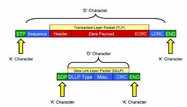
Fig 3: TLP and DLLP Packet Framing with Start and End Control Characters
1.2.1.2.3 Ordered-Sets
Ordered-Sets are multiples of 4 character sequences that starts with a comma (COM) control character followed by other characters. They are transmitted during special events.
• During Link training, Training Sequence 1 and 2 ( TS1 and TS2 ) Ordered-Sets are transmitted over the Link. Link training occurs after fundamental reset, hot reset, or after certain error conditions occur.
• At periodic intervals, the Mux gates the SKIP Ordered-Set pattern through to the Byte Striping logic to facilitate clock tolerance compensation in the receiver circuit of the port at the other end of the Link.
• When a device wants to place its transmitter in the electrical Idle state, it must inform the remote receiver at the other end of the Link. The device gates an electrical Idle Ordered-Set to do so.
• When a device wants to change the Link power state from L0s low power state to the L0 full-on power state, it transmits Fast Training Sequence (FTS) Ordered-Sets to the receiver.
1.2.1.2.4 Logical Idle Sequence .
When there are no packets to transmit on the Link (referred to as Logical Idle Link), rather than leave the Link in a floating state or drive nothing, logical Idle characters are gated.
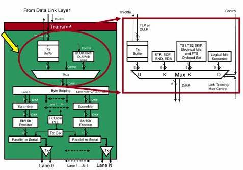
Fig: 4 Transmit Logic Multiplexer
1.2.1.2.5 Implemented Specifications
• Has three inputs ( Control , Control_Character , Data_Character_ from_ Tx_buffer )
• Has two outputs (Control (#D / #K), Data)
• If Control is 1, it sends Data_Character from Tx-buffer , else sends Control_Character.
• Before transferring any packet, Control is set 0 to send STP or SDP
• Then follows data from Tx-buffer when Control is set 1.
• When Packet_End is set by Tx_Buffer, Control is reset to 0 and End character is sent.
• End is common end character for both TLP and DLLP.
1.2.1.3 Byte Striping (Optional)
When a port implements more than one data Lane (i.e., more than one serial data path on the external Link), the packet data is striped across the 2, 4, 8, 12, 16, or 32 Lanes by the Byte Striping logic.
1.2.1.4 Scrambler
The Scrambler eliminates generation of repetitive patterns on a transmitted data stream. Repetitive patterns result in large amount of energy concentrated in discrete frequencies which results in significant EMI noise generated. By scrambling the transmitted data, repetitive patternssuch as 10101010are eliminated. As a result, no single frequency component of the signal is transmitted for significant periods of time. Thus the radiated EMI energy of a transmission is spread over a range in the frequency spectrum. This technique referred to as 'spread spectrum' effectively 'whitens' the frequency content of a signal and reduces the radiated power at any particular frequency.
1.2.1.4.1 Implemented Specifications
• Scrambler algorithm uses LFSR (linear feedback shift register) to generate the random number that doesn't have same frequency of 0's and 1's.
• Number with constant frequency : 1010101010, 111111111, 000000000. etc
• Number with random frequency : 1110101101, 111001011, 001110101, etc.
• Only data characters are processed by Scrambler. Control characters are pre-defined characters and do not required to be processed by Scrambler as they have random frequency.
• If the control character is COM then LFSR value is initialized to ffffh.
• If the control character is SKP then LFSR value is left as it is and SKP is returned by the algorithm.
• If the data sent to scrambler is participated in Training Sequence then the data is not scrambled. Presence of Training Sequence is indicated by Boolean variable Training Sequence . If it is true then the data is not scrambled.
• The outbyte from scrambler is obtained by Xoring the LFSR value with inbyte.
Inbyte: 0 1 2 3 4 5 6 7
XOR
LFSR: 15 14 13 12 12 11 10 9
------------------------------------------------------------------
Oubyte: 0 1 2 3 4 5 6 7
• After Outbyte is calculated LFSR value is shifted 8 clock signals as shown below:
The XOR required to advance 8 bits/clock is:
Bit 0 1 2 3 4 5 6 7 8 9 10 11 12 13 14 15
8 9 10 11 12 13 14 15 0 1 2 3 4 5 6 7
8 9 10 11 12 13 14 15
8 9 10 11 12 13 14 15
8 9 10 11 12 13 14 15
1.2.1.5 8b/10b Encoding
The primary purpose of this scheme is to embed a clock into the serial bit stream transmitted on all Lanes. No clock is therefore transmitted along with the serial data bit stream. This eliminates the need for a high frequency 2.5GHz clock signal on the Link which would generate significant EMI noise and would be a challenge to route on a standard FR4 board. Two devices are connected by simply wiring their Lanes together.
1.2.1.5.1 Advantages
• Creates sufficient 0-to-1 and 1-to-0 transition density (i.e., signal changes) to facilitate re-creation of the receive clock on the receiver end using a PLL.
• Permits the encoding of special control ('K') characters such as the Start and End framing characters at the start and end of TLPs and DLLPs.
• A receiver can check for 'running disparity' errors, or the reception of invalid symbols. Via the running disparity mechanism the data bit stream transmitted maintains a balance of 1s and 0s.
1.2.1.5.2 Disadvantage
Due to the expansion of each 8-bit character into a 10-bit symbol prior to transmission, the actual transmission performance is degraded by 25% or said another way, the transmission overhead is increased by 25%
1.2.1.5.3 Implemented Specifications
• Both Data character and Control characters are encoded.
• Input is outbyte (8-bits) from scrambler.
• Output is 10-bit value.
• The outbyte is split into two parts. One with 5-bit and the other with 3-bit.Then the 5-bit and 3-bit value is compared with lookup table to calculate the corresponding 6-bit and 4-bit value. 10-bit code is obtained by concatenating 6-bit and 4-bit value.
• CRD (current running disparity) value is inspected before converting 5-bit and 3-bit value to 6-bit and 4-bit code.
• CRD can be initialized to either 0 or 1. In the process, if the difference between number of 1's and number of 0's in encoded 10-bit value is positive, CRD's next value is set to 1 (i.e. positive). If the difference is negative then CRD's next value is 0 (i.e. negative). If the difference is 0 then there is no change in CRD value.
• CRD value indicates the balance between the number of 1's and 0's transmitted through the lane. Hence, the circuit the signal from transmitter to receiver is DC balanced.
• The look-up table is shown below:
Table:1 5-bit to 6-bit Encode Table for Data Characters
Data Byte Name |
Unencoded Bits EDCBA |
Current RD abcdei |
Current RD + abcdei |
D0 |
00000 |
100111 |
011000 |
D1 |
00001 |
011101 |
100010 |
D2 |
00010 |
101101 |
010010 |
D3 |
00011 |
110001 |
110001 |
D4 |
00100 |
110101 |
001010 |
D5 |
00101 |
101001 |
101001 |
D6 |
00110 |
011001 |
011001 |
D7 |
00111 |
111000 |
000111 |
D8 |
01000 |
111001 |
000110 |
D9 |
01001 |
100101 |
100101 |
D10 |
01010 |
010101 |
010101 |
D11 |
01011 |
110100 |
110100 |
D12 |
01100 |
001101 |
001101 |
D13 |
01101 |
101100 |
101100 |
D14 |
01110 |
011100 |
011100 |
D15 |
01111 |
010111 |
101000 |
D16 |
10000 |
011011 |
100100 |
D17 |
10001 |
100011 |
100011 |
D18 |
10010 |
010011 |
010011 |
D19 |
10011 |
110010 |
110010 |
D20 |
10100 |
001011 |
001011 |
D21 |
10101 |
101010 |
101010 |
D22 |
10110 |
011010 |
011010 |
D23 |
10111 |
111010 |
000101 |
D24 |
11000 |
110011 |
001100 |
D25 |
11001 |
100110 |
100110 |
D26 |
11010 |
010110 |
010110 |
D27 |
11011 |
110110 |
001001 |
D28 |
11100 |
001110 |
001110 |
D29 |
11101 |
101110 |
010001 |
D30 |
11110 |
011110 |
100001 |
D31 |
11111 |
101011 |
010100 |
Table: 2 5-bit to 6-bit Encode Table for Control Characters
Data Byte Name |
Unencoded Bits EDCBA |
Current RD abcdei |
Current RD + abcdei |
K28 |
11100 |
001111 |
110000 |
K23 |
10111 |
111010 |
000101 |
K27 |
11011 |
110110 |
001001 |
K29 |
11101 |
101110 |
010001 |
K30 |
11110 |
011110 |
100001 |
Table 3. 3-bit to 4-bit Encode Table for Data Characters
Data Byte Name |
Unencoded Bits HGF |
Current RD - fghj |
Current RD + fghj |
--.0 |
000 |
1011 |
0100 |
--.1 |
001 |
1001 |
1001 |
--.2 |
010 |
0101 |
0101 |
--.3 |
011 |
1100 |
0011 |
--.4 |
100 |
1101 |
0010 |
--.5 |
101 |
1010 |
1010 |
--.6 |
110 |
0110 |
0110 |
--.7 |
111 |
1110/0111 |
0001/1000 |
Table 4. 3-bit to 4-bit Encode Table for Control Characters
Data Byte Name |
Unencoded Bits HGF |
Current RD fghj |
Current RD + fghj |
--.0 |
000 |
1011 |
0100 |
--.1 |
001 |
0110 |
1001 |
--.2 |
010 |
1010 |
0101 |
--.3 |
011 |
1100 |
0011 |
--.4 |
100 |
1101 |
0010 |
--.5 |
101 |
0101 |
1010 |
--.6 |
110 |
1001 |
0110 |
--.7 |
111 |
0111 |
1000 |
1.2.1.6 Parallel-to-Serial Converter (Serializer)
The Parallel-to-Serial converter clocks 10-bit symbols out in the bit order 'abcdeifghj', with the least significant bit (a) shifted out first and the most significant bit (j) shifted out last.
1.2.1.6.1 Implementation Specification
• Parallel to serial shift register logic is used here.
1.3 Receive Logic
The receive logic clocks in a serial bit stream arriving on the Lanes of the Link with a clock that is recovered from the incoming bit stream. The receive logic converts the serial bit steam into a parallel symbol stream, processes the incoming symbols, assembles packets and sends them to the Data Link Layer. Receive logic is comprised of:
• The differential receiver.
• The Rx Clock recovery logic.
• The COM symbol and Ordered-Set detector.
• The Serial-to-Parallel converter (Deserializer).
• The Lane-to-Lane De-Skew logic (delay circuit).
• The Elastic Buffer and Clock Tolerance Compensation logic.
• The 10bit-to-8bit decoder.
• The De-scrambler.
• The Byte-Unstriping logic
• The Demultiplexer (Demux)
• The Receive Buffer.
We've implemented it partially with the functionality for:
• The Serial-to-Parallel converter (Deserializer).
• The COM symbol and Ordered-Set detector.
• The 10bit-to-8bit decoder.
• The Error Detector
• The Descrambler.
• The Demux
• The Receive Buffer.
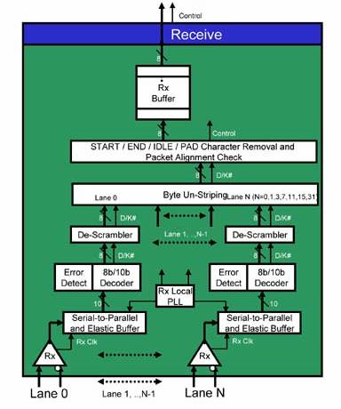
Fig 5: Physical Layer Receive Logic Details
1.3.1 Serial-to-Parallel converter (Deserializer)
The incoming serial data on each lane is converted into parallel data by deserializer.
1.3.1.1 Implementation Specifications
• Converts serial bit into parallel using algorithm for serial to parallel shift register
• The clock is implemented internally.
• The converter waits for all serial bits and stores output of shift register into register parallel_output of width 10bits.
1.3.2 The COM symbol and Ordered-Set detector
The 10-bit encoding of the COM symbol contains two bits of one polarity followed by five bits of the opposite polarity. Unless an error occurs, no other character has this property, thereby making it easily detectable.
1.3.2.1 Implementation Specification
• It is embedded into 10bit-to-8bit decoder
• When COM symbol and Ordered-Set or any other control characters are encountered, comparing with corresponding 10 bit values for control characters recognizes them. It's easy to do that because there are only 8 such characters with predefined code.
1.3.3 Error Detector
• It is also embedded into 10bit-to-8bit decoder.
• Error in transmission of data is detected by comparing the number of 1's and 0's in 10-bit symbol obtained from serial-to-parallel converter. If the difference is more than one then there is error and data is reported to be corrupted.
• Error can also be traced by comparing the number of 1's and 0's in 6-bit and 4-bit value of 10-bit symbol.
• Maximum number of 1's or 0's allowed in 6-bit value is 4.
• Maximum number of 1's or 0's allowed in 4-bit value is 3.
If any of the above rules are violated then the data is reported to be corrupted.
This is the first stage of error detection in receiver device and reports critical error in data transmission.
1.3.4 8b/10b Decoder
The 8b/10b Decoder uses two lookup tables (the D and K tables) to decode the 10-bit symbol stream into 8-bit Data (D) or Control (K) characters plus the D/K# signal. The state of the D/K# signal indicates that the received symbol is:
• A Data (D) character if a match for the received symbol is discovered in the D table. D/K# is driven High.
• A Control (K) character if a match for the received symbol is discovered in the K table. D/K# is driven Low.
1.3.4.1 Implementation Specification
• Both Data character and Control characters are encoded.
• Input is 10 bit value from serial-to-parallel converter.
• Output is 8-bit decoded value and control character to indicate whether the decoded value is a data character or control character.
• It embeds COM symbol and Ordered-Set detector, control character detector and error detector.
• Input is parallel_output (10-bits) from serial to parallel converter.
• Output is 8-bit value.
• The parallel_output is compared with standard 10-bit encoded codes for detecting Control Character . The 6-bit and 4-bit segments of parallel_output are then compared with the look-up tables and are correspondingly converted to 5-bit and 3-bit values. The output from 8bit-to-10bit decoder is, then, obtained by concatenating 5-bit and 3-bit values
• CRD (current running disparity) value is inspected before converting 5-bit and 3-bit value to 6-bit and 4-bit code.
• CRD can be initialized to either 0 or 1. In the process, if the difference between number of 1's and number of 0's in encoded 10-bit value is positive, CRD's next value is set to 1 (i.e. positive). If the difference is negative then CRD's next value is 0 (i.e. negative). If the difference is 0 then there is no change in CRD value.
• CRD value indicates the balance between the number of 1's and 0's transmitted through the lane. Hence, the circuit the signal from transmitter to receiver is DC balanced.
• The look-up table is same as in 8bit-to-10bit encoder.
1.3.5 De scrambler
The De-Scrambler only de-scrambles Data (D) characters associated with a TLP or DLLP (D/K# is high). The De-scrambler descrambles the random code generated by scrambler into the exact 8-bit code contained in packet obtained from Data link layer.
1.3.5.1 Implementation Specification
• De-scrambler algorithm is very similar to scrambler.
• De-scrambler algorithm uses LFSR (linear feedback shift register) to recover the original 8-bit character from random number that doesn't have same frequency of 0's and 1's.
• Only data characters are processed by De-scrambler algorithm is very similar to scrambler. Control characters are pre-defined characters and do not required to be processed by De-scrambler as they are untouched by scrambler.
• If the control character is COM then LFSR value is initialized to ffffh.
• If the control character is SKP then LFSR value is left as it is and the algorithm returns SKP.
• If the data sent to De-scrambler is participated in Training Sequence then the data is not unscrambled. Boolean variable Trainiing_Sequence indicates presence of Training Sequence. If it is true then the data is not unscrambled.
• The outbyte from De-scrambler is obtained by Xoring the LFSR value withinbyte.
Inbyte: 0 1 2 3 4 5 6 7
XOR
LFSR: 15 14 13 12 12 11 10 9

Oubyte: 0 1 2 3 4 5 6 7
• After Outbyte is calculated LFSR value is shifted 8 clock signals as shown below:
The XOR required to advance 8 bits/clock is:
Bit 0 1 2 3 4 5 6 7 8 9 10 11 12 13 14 15
8 9 10 11 12 13 14 15 0 1 2 3 4 5 6 7
8 9 10 11 12 13 14 15
8 9 10 11 12 13 14 15
8 9 10 11 12 13 14 15
1.3.6 Demultiplexer (Demux)
1.3.6.1 Implementation Specifications
• It separates the control characters and data characters based on the Control signal sent by De-scrambler.
• Inputs are Control signal and Character from De-scrambler;
• Outputs are Contro l signal , Data_Character and Control_Character .
• If Control is set to 1, Data_character is sent to the receiver buffer but if it is 0 then the control_character is received within the physical layer module and not passed to any further module.
1.3.7 Receive Buffer (Rx Buffer)
1.3.7.1 Implementation Specification
• It restores the data stored in transmit buffer of physical layer of transmitter.
• Inputs are Control singnal and Data_Character
• Output is Data_character.
• If Control Signal is 1 then the Data_Character received form Demux is stored in Receiver Buffer. This data is finally sent to Data Link Layer.