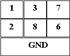
BITX
We describe here our adventure building the BITX, we will also speak about how to move it to other bands.
The BITX was a project blessed by a lot of hams from several countries. They built it and spoke very well about the results.
The BITX was originally designed by the indian ham Ashhar Farhan and it was shown to the world after its big use in the Tsunami disaster which swept the indian coast. The CNN report with the interview with Farhan building the BITX can be seen in the yahoo group BITX20
http://groups.yahoo.com/group/BITX20/
running since 2004 and with over 200 members.
The BITX20 schematic and construction details for 20m can be obtained in:
http://www.phonestack.com/farhan/bitx.html
The details about how to select the cristals and how to calculate the SSB filter can be obtained in:
http://www.phonestack.com/farhan/xcvr1.html
The comments and mods can be seen in:
http://groups.yahoo.com/group/BITX20/files/
===================================
How to change the BITX bands
VFO Frequency
The VFO frequency is obtained adding or substacting the segment of frequencies to be covered to the IF (10MHz).
Ex 40m 7000 to 7300kHz
We will have
10000 + 7000 = 17000
to
10000 +7300 = 17300
VFO covering from 17000 to 17300kHz
OR
10000 - 7000 = 3000
to
10000 - 7300 = 2700
VFO covering from 2700 to 3000kHz
IMPORTANT
Check always if the VFO frequency multiplied by an integer number is not close or equal to the range of in band frequency covered or to the IF. (ex VFO in 3580 for 40 is not correct as 2x3580=7160). The ideal way would be using a VFO frequency bigger than half the maximal in band frequency and the IF.
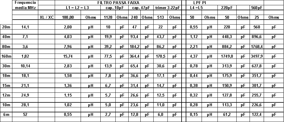
For the COILS L1, L2, L3, L4, L5 and associated capacitors, calculate the individual capacitive or inductive reactance for 20m and after we have the reactance figured out, calculate the part value changing the frequency to the desired band.
Table:
The table values are the calculated ones, and must be adjusted as needed, especially the capacitors which must use commercial values.
The LPF inductor (PI filter) must be kept.
When we build the BITX for 40m, we change the passband filter inductors to 4,7�H (4,03 in the table), a commercial value we had on hand during the construction.
================================
Building the BITX
The ideal way is beginning by the most difficult and work requiring section:
The SSB filter
This is a very critical filter, as it removes one of the DSB sidebands, allowing pass only to the other band.
Purchase from 10 to 20 10MHz crystals, which must be from the same manufacturer and preferably from the same batch. These crystals can be found by about R$0,50 (U$0,20) in the commerce.
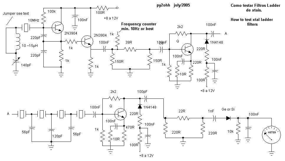
Build the test circuit as described in:
http://www.phonestack.com/farhan/xcvr1.html
Our construction:
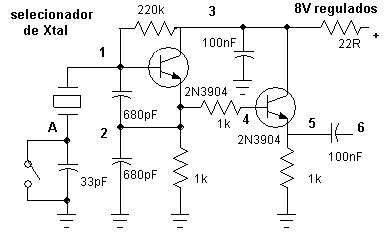
Schematic
Layout - 18 x 30mm board
The 680pF capacitors must be of styroflex or NP0 association.
The key which shorts the 33pF capacitor is made with a surplus part wire.
The construction is not critical, the 8V regulated supply can come from a zener, 78L08 or 7808.
Label the crystals on the top side, that avoids too much handling.
Test the crystals in the above circuit, measure the frequency with a frequency counter with 10 Hz precission or better, take note.
Short the 33pF capacitor and measure again, take note of the new frequency.
The chosen crystals must be in a 60 Hz range between them in both measurings.
Practical results for our measurings:
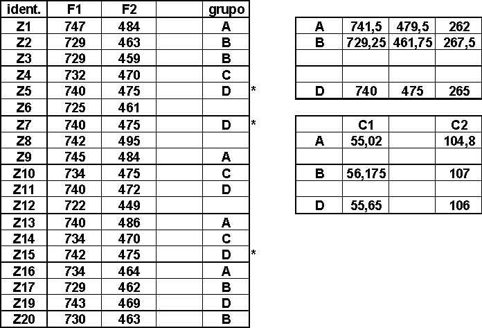
Note: the measurings were made with a frequency counter with a minimal display of 10Hz. This way the 747 reading must be understood as 9,991,470 Hz.
Nota : as medi��es foram feitas com um frequenc�metro com indica��o m�nima de 10Hz. Assim a leitura de 747 deve ser entendida como 9.997.470 Hz.
We add the values from each type of reading from each group, look for the mean between F1 and F2, we calculate the maximum frequency deviation and referring the BITX designer the C1 capacitor value will be 21 x mean deviation (in KHz) and C2 40 x mean deviation.
For the D group we choose the lower variation.
Realize that in the A group se have Z1 and Z13 with a 70Hz variation in the F1 reading.
We will use a 56pF NP0 for C1 and 120pF for C2 (they're already rounded to commercial values).
====================================
We are now going to build the bidirectional amplifier modules, so we will be able to analyze our filter.
Bidirectional amplifiers:
In the BITX we have 6 bidirectional amplifiers (we refer them here by the transistor QX identification in the schematic), the same circuit, being identical 4 of them (Q1, Q2, Q13 and Q12) and two of them with small differences (Q3 and Q11).
The circuit
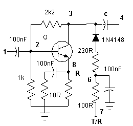
The board
Q1, Q2, Q13 and Q12 modules
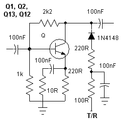
ceramic 100nF (.1�F), 1/8 or 1/4W resistors, 2N2222, 2N3904, BC547B or C, BC548B or C, BC107 transistors.
I used the BF240.
In order to mount correctly your transistor, we recommend looking for the datasheet in the WEB, looking for "2N2222.pdf" in Google as an example.
The C capacitor (100nF, .1�F) is mounted afterwards.
Mounting sequence: Tr, 2K2, 220R e (emitter), 100R e, 100nF (.1�F) e, diode, 220R c (collector), 100R +, 1K b.
Test: enter a RF signal (25MHz in our case), shunted with a 50R resistor, with a 200mVp level. We obtain almost 1.5Vp in the output.
Q3 module
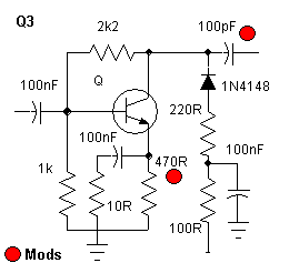
In this module we have the 470R resistor and the 100pF output capacitor departing from the previous values.
Q11 module
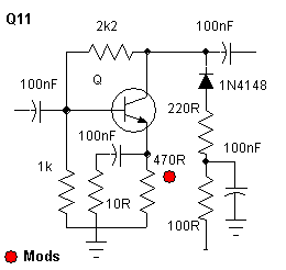
In this module only the 47R resistor is different.
Building the bidirectionals:
Mount the Q13 (TX black - above) with Q1 (RX red - under) pairs.
Important: 100nF (.1�F) ceramic capacitors must be mounted between the islands 1 and 3 in both modules, coresponding to that connected between islands 3 and 4 in the schematic.
Mount the Q12 (TX black - above) with Q2 (RX red - under) pair.
Important: 100nF (.1�F) ceramic capacitors must be mounted between the islands 1 and 3 in both modules, coresponding to that connected between islands 3 and 4 in the schematic.
Mount the Q11 (TX black - above -this has the 470R resistor) with Q3 (RX red - in the bottom, this has the 100pF capaacitor and the 470R resistor).
Important: 100nF (.1�F) ceramic capacitors must be mounted between the islands 1 and 3 in both modules, coresponding to that connected between islands 3 and 4 in the schematic.
========================================
Crystal filter building
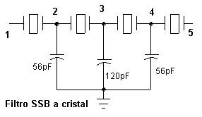
Filter schematic
The filters were chosen following the already described procedure, as the capacitors calculation.
Filter mounting board:
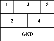
Layout
==========================================
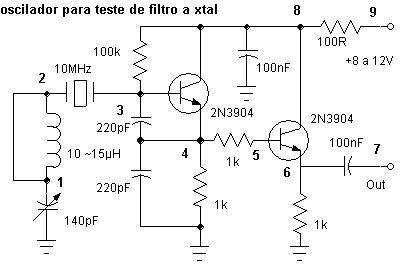
Building the oscillator to test the filter
For we to test the filter the simplest way is putting a signal generator in the input and measure the RF voltage in the output and drawing a graph.
As a very stable oscillator with a span of some 20KHz, we will build it from the BFO oscillator in the BITX an oscillator with these features.
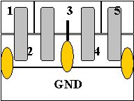
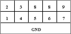
Suggested layout
In order to obtain frequencies above the crystal nominal one, a jumper must be soldered between the islands 1 an 2, short circuiting the inductor.
The frecuencies under the crystal nominal one are achieved with the inductor in series with the capacitor (without a short circuit wire-jumper).
========================================
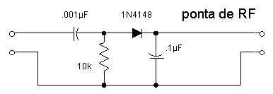
Besides for a simple filter test it is necessary an RF probe, that will measure the RF peak voltage.
RF PROBE
The voltmeters show a lot of problems when measuring alternating current when the frequency is over 200 Hz.
In order to measure in high frequency we need an adapter.
The adapter or rf probe described here converts the rf in a direct current that can be read in a conventional voltmeter (analogic or digital).
A rf probe is very useful in adjustments, mounting processes, tests and rf measurings in general (power, swr, etc.).
Schematic
Parts list
01 1000pF or .001 or 102 50 Volt ceramic capacitor
01 1N4148 or 1N914 signal diode; ideally OA49, OA80 or OA79 or 1N34 (bigger in size)
01 10,000 Ohms 1/8 W or more resistor
01 .1�F or 104 50 Volt or more ceramic or poliester capacitor.
01 RCA female connector
01 aluminium tube (see text)
01 probe point (see text)
Construction
We use an 18mm by 12mm unetched printed circuit board cut in the following way:
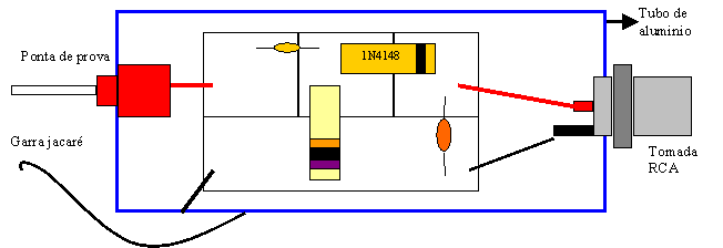
The tube was got from surplus with 20mm diameter and two plastic end covers, some time ago we had aluminum tubes as containers of C vitamins that would serve for this use very well... Nothing prevents any other format.
As a probing point I used a polimeter surplus whith the plastic part broken (he who keeps it, have it), but for R$1,00 we bought two new points in the shop.
The point goes in the tube closed side, the end cover goes to the RCA jack. The internal ground is connected to the tube and the crocodile jack too, with a 10 cm wire.
The circuit must be internally isolated, we used small plastic bags.
We used a male RCA jack for the output, with two coloured cocrodile jacks and coloured wires for connection to the polimeter.
In the case we desire it, in order to measure lower frequencies (i.e. audio) the 1000pF capacitor must be increased according with the frequency.
The reading must be increased in 0.7 Volts (0.4 Volts for germanium diodes).
Mode of use:
Directly to measure RF voltages, the values is in peak Volts Vp, that is half the value of the peak to peak voltage Vpp and 1.41 times lower than the RMS voltage Vrms.
1 peak Volts=(0.5 x peak-to-peak Volts)=0.7 x RMS Volts
1Vp =0,5 Vpp=0,7Vrms
===========================================
Before testing the filter we need to establish the filter input and output impedances.
For this we did two 50 ohms impedance input and output attenuator.
The crystal filter impedance is 200 Ohms.
That way the IF amplifier input must "see" 50 Ohms. The IF amplifier output must also "see" 50 Ohms.
The theory and the discussion about there impedances can be found in the original article (see link in this site).
We have a spreadsheet for calculation of other attenuators in this site.
Schematic
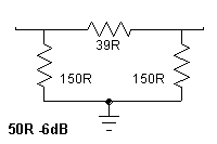
The other attenuator is similar but it is of 50R -3dB and it is already used in the same BITX, the resistors are 2 x 220R and 22R.
======================================
How to measure the filter performance
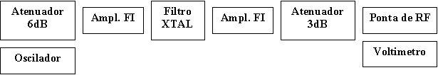
Block diagram
Schematic
IMPORTANT :
In spite of not being in the schematic, the bidirectional amplifiers must be completed with both modules mounted and grounded, as there is an RF feedback in the circuit even being unconnected.
This work has to be done again, because we didn't regarded of this fact.
For any doubt, write a Email.
Procedure:
See the example:
|
Hz |
mVp |
|
9.992.330 |
10 |
|
9.993.230 |
50 |
|
9.993.500 |
100 |
|
9.993.690 |
150 |
|
9.993.890 |
200 |
|
9.994.080 |
250 |
|
9.994.230 |
300 |
|
9.994.310 |
350 |
|
9.994.400 |
400 |
|
9.994.470 |
470 |
|
9.994.640 |
600 |
|
9.994.710 |
650 |
|
9.995.690 |
688 |
|
9.997.160 |
650 |
|
9.997.330 |
470 |
|
9.997.390 |
400 |
|
9.997.430 |
350 |
|
9.997.470 |
300 |
|
9.997.530 |
250 |
|
9.997.620 |
200 |
|
9.997.730 |
150 |
|
9.997.820 |
100 |
|
9.998.000 |
50 |
|
9.998.600 |
10 |
Graph made using Excel.
Another filter (with other crystals) with 100pF - 120pF - 100pF capacitors resulted in this graph:
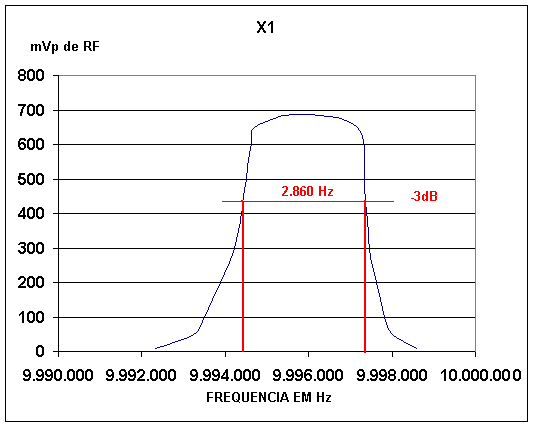
The -3dB line is at 70% of the maximum mean measured value.
The passband width value in a SSB filter must be between 2.5kHz and 3.5kHz.
In order to use the filter in LSB ou lower side band the beat frequency oscillator (BFO or OFB in portuguese) signal must be in the upper part of the filter, close to the red line on the right side of the graph. In this way the lower frequencies will pass following the filter characteristics.
For USB or Upper Side Band the beat frequency oscillator signal must be in the lower part of the passband, close to the red line on the lefrt side of the graph. This way only the upper frequencies will pass following the filter characteristics.
For CW the beat frequency oscillator tuning follows that suggested for LSB.
In the graph example, the oscillator tuned to 9,337,300 Hz will pass frequencies between 9,997,330 - 9,994,470 = 2,860 and 9,997,300 - 3,997,300 = 0 Hz, that is, the lower side band.
As discussed in the J. A. Hardcastle, G3JIR, article, knowing the passband width of a filter we can recompute the capacitors for a desired passband using the ratio:
C ? / C1 = ( BW1 / BW? )^2
Where C1 is the capacitor initial value and C? is the desired value and BW1 the passband initial value and BW? the desired value of the passband.
When bigger the capacitor values, narrower will be the passband, and the capacitors will be able to be modified to correct or modify the passband width or shape.
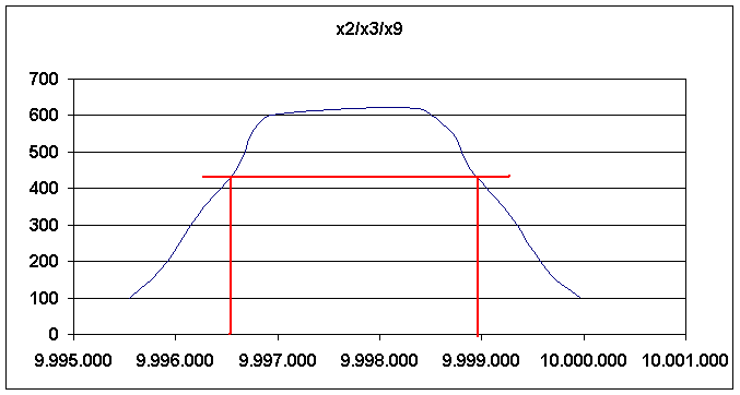
Graph for another filter - 100 - 22 - 100 pF capacitors
We will soon describe another way to measure the filter passband, using the sound board in a PC and a white noise generator. The passband picture is instantaneous and very practical.
BITX
Descreveremos aqui nossa aventura montando o BITX, tamb�m falaremos de como altera-lo para outras faixas.
O BITX foi um projeto consagrado por muitos colegas de diversos pa�ses que montaram e falam muito bem dos resultados obtidos.
O BITX foi originalmente projetado pelo colega indiano Ashar Farhan e foi consagrado mundialmente ap�s a grande utiliza��o dele no desastre do Tsunami que varreu a costa indiana. A reportagem da CNN com a entrevista do Fahran montando BITX pode ser vista no Grupo BITX20 do Yahoo
http://groups.yahoo.com/group/BITX20/
que existe desde 2004 e conta com mais de 200 membros.
O esquema e detalhes da constru��o do BITX20, para 20m pode ser obtido em :
http://www.phonestack.com/farhan/bitx.html
Os detalhes de como selecionar os cristais e como calcular o filtro para SSB podem ser obtidos em :
http://www.phonestack.com/farhan/xcvr1.html
Os coment�rios, modifica��es podem ser vistos em :
http://groups.yahoo.com/group/BITX20/files/
===================================
Como alterar as bandas do BITX
Freq��ncia do VFO
A freq��ncia do VFO � obtida somando ou subtraindo a faixa de freq��ncias a ser coberta, com a freq��ncia de FI (10MHZ).
Ex 40m 7000 a 7300kHz
Teremos
10000 + 7000 = 17000
a
10000 +7300 = 17300
VFO cobrindo de 17000 a 17300kHz
OU
10000 - 7000 = 3000
a
10000 - 7300 = 2700
VFO cobrindo de 2700 a 3000kHz
IMPORTANTE
Verifique sempre se a freq��ncia do VFO multiplicada por um numero inteiro n�o fica pr�xima ou igual a freq��ncia de cobertura da faixa ou da freq��ncia do FI. (ex VFO em 3580 para 40m n�o � correto pois 2x3580= 7160 ). O ideal seria utilizar a freq��ncia do VFO superior a metade da freq��ncia m�xima de cobertura e da freq��ncia do FI.
BOBINAS L1, L2, L3, L4, L5 e capacitores associados calcular a reat�ncia capacitiva ou indutiva individual para 20m e ap�s a reat�ncia calculada calcular o valor do componente alterando a freq��ncia para a faixa desejada.
Tabela :
Os valores da tabela s�o os calculados, e devem ser ajustados conforme a necessidade, principalmente os capacitores que devem ser comerciais.
O indutor do LPF (filtro PI) deve ser mantido.
Quando montamos o BITX 40m, alteramos os indutores do filtro passa faixa para 4,7�H (4,03 na tabela), valor comercial que disp�nhamos na ocasi�o da montagem.
================================
Montando o BITX
O ideal � iniciar pela parte mais trabalhosa e dif�cil :
O Filtro de SSB
Este filtro � muito critico, pois ele retira uma das bandas do sinal de DSB, deixando passar somente a outra banda.
Adquira de 10 a 20 cristais de 10MHz, que devem ser do mesmo fabricante e preferencialmente do mesmo lote. Estes cristais podem ser encontrados por cerca de R$0,50 (U$0,20) no comercio.
Monte o circuito descrito de teste conforme descrito em :
http://www.phonestack.com/farhan/xcvr1.html
Nossa montagem :
Esquema
Layout - placa de 18 x 30mm
Os capacitores de 680pF deve ser de styroflex ou uma associa��o de capacitores NP0.
A chave que curtocircuita o capacitor de 33pF e feita com uma sobra de lide de componente.
A montagem n�o � critica, a tens�o de 8V regulados podem vir de um zener, 78L08 ou 7808.
Identificar os cristais no topo, que evita sair no manuseio.
Testar os cristais no circuito acima, medir a freq��ncia com um frequenc�metro com precis�o de 10Hz ou melhor, anotar.
Curtocircuitar o capacitor de 33pF e medir novamente, anotar a nova freq��ncia.
Os cristais escolhidos devem estar dentro de uma varia��o m�xima entre eles de 60Hz nas duas medi��es.
Resultado pratico de nossas medi��es :
Nota : as medi��es foram feitas com um frequenc�metro com indica��o m�nima de 10Hz. Assim a leitura de 747 deve ser entendida como 9.997.470 Hz.
Somamos os valores de cada tipo de leitura de cada grupo, achamos a media de F1 e de F2, calculamos o desvio m�dio de freq��ncia e segundo o autor do BITX o valor do capacitor C1 ser� dado por 21 x media de desvio (em kHz) e C2 por 40 x a media de desvio.
Para o grupo D escolhemos a menor varia��o.
Note que no grupo A temos Z1 e Z13 tendo uma varia��o de 70Hz na leitura F1.
Adotaremos como C1 o valor de 56pF NP0 e para C2 120pF (j� arredondados e com valores comerciais).
====================================
Vamos agora construir os m�dulos dos amplificadores bidirecionais, assim poderemos analisar nosso filtro.
Amplificadores bidirecionais :
No BITX temos 6 amplificadores bidirecionais (aqui tratamos pela identifica��o no esquema do transistor Qx), o mesmo circuito : sendo 4 id�nticos (Q1, Q2, Q13 e Q12) e dois com pequenas diferen�as (Q3 e Q11).
O circuito
A placa
M�dulos Q1, Q2, Q13 e Q12
100nF cer�mico, resistores de 1/8 ou 1/4W, transistores 2N2222, 2N3904, BC547B ou C, BC548B ou C, BC107.
Eu utilizei o BF240.
Para montar corretamente seu transistor recomendamos procurar o datasheet na WEB, procurando por exemplo "2n2222.pdf" no Google.
O capacitor C neste caso de 100nF � montado depois.
Seq��ncia de montagem : Tr, 2k2, 220R e (emissor), 100R e, 100nf e, diodo, 220R c (coletor), 100R +, 1K b.
Teste : entrar com um sinal de RF (nosso caso 25MHz), shuntado com um resistor de 50R, com n�vel de 200mVp . obtemos na sa�da cerca de 1,5Vp.
Modulo Q3
Neste modulo temos o resistor de 470R e o capacitor na sa�da de 100pF diferentes.
Modulo Q11
Neste modulo apenas o resistor de 470R � diferente.
Montando os bidirecionais :
Monte os pares Q13 (Tx preto - superior) com Q1 (Rx vermelho - em baixo).
Importante : entre as ilhas 1 e 3 de ambos os m�dulos dever�o ser soldados capacitores de 100nF (cer�micos) correspondentes ao conectado entre ilha 3 e 4 no esquema.
Monte os pares Q12 (Tx preto - superior) com Q2 (Rx vermelho - em baixo).
Importante : entre as ilhas 1 e 3 de ambos os m�dulos dever�o ser soldados capacitores de 100nF (cer�micos) correspondentes ao conectado entre ilha 3 e 4 no esquema.
Monte os pares Q11 (Tx preto - superior - este tem resistor de 470R) com Q3 (Rx vermelho - em baixo este tem o capacitor de 100pF e o resistor de 470R).
Importante : entre as ilhas 1 e 3 de ambos os m�dulos dever�o ser soldados capacitores de 100nF (cer�micos) correspondentes ao conectado entre ilha 3 e 4 no esquema.
========================================
Montagem do filtro a cristal
Esquema do filtro
Os filtros foram escolhidos conforme procedimento j� descrito, bem como o calculo dos capacitores.
Placa para montagem do filtro :
Layout
==========================================
Montagem do oscilador para teste do filtro
Para testarmos o filtro a forma mais simples � a de colocarmos um gerador de sinais na entrada e medir a tens�o de RF de sa�da, e construir um gr�fico.
Como � necess�rio um oscilador muito est�vel e com uma varia��o de cerca de 20kHz, vamos montar a partir do oscilador BFO do BITX um oscilador com estas caracter�sticas.
Layout sugerido
Para se obter freq��ncias acima da normal do cristal dever� ser soldado um jumper da ilha 1 a ilha 2, colocando o indutor em curto circuito.
As freq��ncias inferiores a da normal do cristal s�o conseguidas com o indutor em serie com o capacitor (sem o fio de curto circuito -jumper).
========================================
Ainda para um teste simples do filtro � necess�rio uma ponta de RF, que vai medir a voltagem de pico de RF.
PONTA DE RF
Os volt�metros apresentam muitos problemas ao se medir corrente alternada quando a freq��ncia passa de 200 Hz.
Para medirmos alta freq��ncia necessitamos de um adaptador.
O adaptador ou ponta de rf aqui descrito converte a rf em corrente cont�nua, que pode ser lida em um volt�metro convencional (anal�gico ou digital).
Uma ponta de rf � muito �til em ajustes, montagens, testes e medi��es de rf em geral (pot�ncia, swr etc.).
Esquema
Materiais
01 capacitor cer�mico de 1000pF ou .001 ou 102 de 50 Volts
01 diodo de sinal 1n4148 ou 1n914; ideal diodo de germ�nio OA49, OA80 ou OA79 (maiores em tamanho)
01 resistor de 10.000 Ohms 1/8 W ou mais
01 capacitor cer�mico ou poli�ster de .1�F ou 104 de 50 Volts ou mais.
01 conector f�mea RCA
01 tubo de alum�nio (ver texto)
01 ponta de prova (ver texto)
Montagem
Utilizamos uma placa de circuito impresso de 18mm por 12 mm, cortada da seguinte forma
O tubo foi conseguido de sucata de 20mm de di�metro com duas tampas pl�sticas, h� algum tempo t�nhamos como embalagem de vitaminas C tubos de alum�nio que serviriam muito bem para o uso (que voltaram �s prateleiras...). Nada impede outros formatos.
Como ponta de prova utilizei uma sucata de mult�metro que a parte pl�stica havia se quebrado (quem guarda tem), mas por R$1,00 compramos duas pontas novas no comercio.
A ponta vai no lado fechado do tubo, na tampa vai a tomada RCA. O terra interno � parafusado na carca�a e a garra jacar� tamb�m, com um fio de uns 10 cm.
O circuito deve ser isolado internamente, utilizamos saquinhos pl�sticos de embalagens.
Para a sa�da utilizamos uma tomada RCA macho, com duas garras jacar� coloridas e fios coloridos para conex�o no mult�metro.
Caso desejado, para medir freq��ncias menores (ex. �udio) o capacitor de 1000pF deve ser aumentado de acordo com a freq��ncia.
As leituras devem ter um acr�scimo de 0,7 Volts (0,4 Volts no caso de diodos de germ�nio).
Utiliza��o :
Diretamente para medir tens�es de RF, o valor � em Volts de pico Vp, que � a metade do valor da tens�o de pico a pico Vpp e 1,41 vezes menor que a tens�o RMS Vrms.
1 Volts pico = (0,5 x Volts pico-a-pico ) = 0,7 x Volts RMS
1Vp =0,5 Vpp=0,7Vrms
===========================================
Antes de testar o filtro precisamos garantir as imped�ncias no filtro de entrada e de sa�da.
Para isto fizemos dois atenuadores de 50 ohms de impedi�ncia de entrada / sa�da.
A impedi�ncia do filtro a cristal � de 200 Ohms.
Assim a entrada do amplificador de FI deve "ver" 50 Ohms. Tamb�m a sa�da do amplificador de FI deve "ver" 50 Ohms.
A teoria como as explica��es sobre estas imped�ncias podem ser encontradas no artigo original (veja link nesta pagina).
Temos uma planilha neste site para calculo de outros atenuadores.
Esquema
O outro atenuador � semelhante mas � de 50R -3dB e j� � utilizado no pr�prio BITX, os resistores s�o 2 x 220R e 22R.
======================================
Como medir o desempenho do Filtro
Diagrama de blocos
Esquema
IMPORTANTE :
Apesar de n�o constarem do esquema, os amplificadores bidirecionais dever�o estar completos com os dois m�dulos montados e aterrados, pois existe uma realimenta��o de RF que age no circuito, mesmo ele estando desligado.
Este trabalho teve que ser refeito, devido n�o atentarmos a este fato.
Qualquer d�vida escreva um Email.
Procedimento :
Veja o exemplo :
|
Hz |
mVp |
|
9.992.330 |
10 |
|
9.993.230 |
50 |
|
9.993.500 |
100 |
|
9.993.690 |
150 |
|
9.993.890 |
200 |
|
9.994.080 |
250 |
|
9.994.230 |
300 |
|
9.994.310 |
350 |
|
9.994.400 |
400 |
|
9.994.470 |
470 |
|
9.994.640 |
600 |
|
9.994.710 |
650 |
|
9.995.690 |
688 |
|
9.997.160 |
650 |
|
9.997.330 |
470 |
|
9.997.390 |
400 |
|
9.997.430 |
350 |
|
9.997.470 |
300 |
|
9.997.530 |
250 |
|
9.997.620 |
200 |
|
9.997.730 |
150 |
|
9.997.820 |
100 |
|
9.998.000 |
50 |
|
9.998.600 |
10 |
Gr�fico feito no Excell.
Outro filtro (com outros xtais) com capacitores de 100pF - 120pF - 100pF resultaram neste gr�fico :
A linha de -3dB esta a 70% do valor m�dio m�ximo
O valor da banda de passagem de um filtro de SSB deve ser de 2,5kHz a 3,5kHz.
Para utilizar o filtro como LSB ou banda lateral inferior o sinal do oscilador de batimento (BFO ou OFB) dever� estar na parte superior do filtro pr�ximo da linha vermelha a direita do gr�fico. Assim as freq��ncias inferiores passar�o segundo as caracter�sticas do filtro.
Para USB ou banda lateral superior o sinal do oscilador de batimento devera estar na parte inferior do filtro, pr�ximo a linha vermelha a esquerda do gr�fico. Assim somente as freq��ncias superiores passar�o segundo as caracter�sticas do filtro.
Para CW o ajuste do oscilador de batimento segue ao recomendado para LSB.
Ex no gr�fico, oscilador em 9.997.300 Hz passar� freq��ncias de 9.997.330 - 9.994.470 = 2.860Hz a 9.997.300 -9.9977.300 = 0Hz ou seja a parte inferior da portadora.
Segundo artigo do colega G3JIR J. A Hardcastle, conhecendo-se a banda de passante de um filtro podemos recalcular os capacitores para uma banda passante desejada e vale a rela��o :
C ? / C1 = ( BW1 / BW? )^2
Onde C1 valor inicial do capacitor e C? valor desejado
E BW1 valor inicial da banda passante e BW? Valor desejado da banda passante.
Quanto maior o valor dos capacitores menor ser� a banda passante, e os capacitores poder�o ser alterados para corre��o ou altera��o da curva de resposta.
Gr�fico de outro filtro - capacitores de 100 - 22 - 100 pF
Descreveremos em breve outra forma de medir a resposta do filtro, utilizando a placa de som de um PC e um gerador de ru�do branco. A visualiza��o da curva � instant�nea e muito pratica.