PCI
During the early 1990s, Intel introduced a new bus standard for consideration, the Peripheral Component Interconnect (PCI) bus. PCI presents a hybrid of sorts between ISA and VL-Bus. It provides direct access to system memory for connected devices, but uses a bridge to connect to the frontside bus and therefore in the CPU. Basically, this means that it is capable of even higher performance than VL-Bus while eliminating the potential for interference with the CPU.
The frontside bus is a physical connection that actually connects the processor to most of the other components in the computer, including main memory ( RAM ), hard drives and the PCI slots. These days, the frontside bus usually operates at 400-MHz, with newer systems running at 800-MHz.
The backside bus is a separate connection between the processor and the Level 2 cache This bus operates at a faster speed than the frontside bus, usually at the same speed as the processor, so all that caching works as efficiently as possible. Backside buses have evolved over the years. In the 1990s, the backside bus was a wire that connected the main processor to an off-chip cache. This cache was actually a separate chip that required expensive memory. Since then, the Level 2 cache has been integrated into the main processor, making processors smaller and cheaper. Since the cache is now on the processor itself, in some ways the backside bus isn't really a bus anymore.
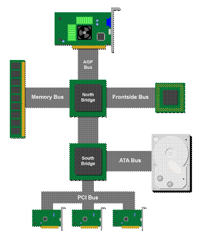
Figure 1
PCI can connect more devices than VL-Bus, up to five external components. Each of the five connectors for an external component can be replaced with two fixed devices on the motherboard . Also, you can have more than one PCI bus on the same computer, although this is rarely done. The PCI bridge chip regulates the speed of the PCI bus independently of the CPU's speed. This provides a higher degree of reliability and ensures that PCI-hardware manufacturers know exactly what to design for PCI originally operated at 33 MHz using a 32-bit-wide path. Revisions to the standard include increasing the speed from 33 MHz to 66 MHz and doubling the bit count to 64. Currently, PCI-X provides for 64-bit transfers at a speed of 133 MHz for an amazing 1-GBps (gigabyte per second) transfer rate!
PCI cards use 47 pins to connect (49 pins for a mastering card, which can control the PCI bus without CPU intervention). The PCI bus is able to work with so few pins because of hardware multiplexing, which means that the device sends more than one signal over a single pin. Also, PCI supports devices that use either 5 volts or 3.3 volts.
Introduction to PCI Bus Operation
Initiator, Target and Agents
There are two participants in every PCI burst transfer: the initiator and the target. The initiator, or bus master, is the device that initiates a transfer. The terms bus master and initiator can be used interchangeably and frequently are in the PCI specification. The target is the device currently addressed by the initiator for the purpose of performing a data transfer. PCI initiator and target devices are commonly referred to as PCI-compliant agents in the spec.
Burst Transfer
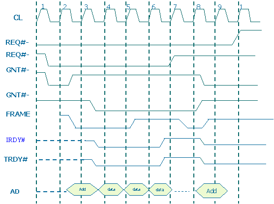
Burst transfer consists of a single address phase followed by two or more data phases. The bus master only has to arbitrate for bus ownership one time. The start address and transaction type are issued during the address phase. All devices on the bus latch the address and transaction type and decode them to determine which is the target device. The target device latches the start address into an address counter (assuming it supports burst mode) and is responsible for incrementing the address from data phase to data phase.
PCI data transfers can be accomplished using burst transfers. Many PCI bus masters and target devices are desiged to support burst mode. It should be noted that a PCI target may be designed such that it can only handle single data phase transactions. When a bus master attempts to perform a burst transaction, the target forces the master to terminate the transaction at the completion of the first data phase. The master must re-arbitrate for the bus to attempt resumption of the burst with the next data item. The target terminates each burst transfer attempt when the first data phase completes. This would yield very poor performance, but may be the correct approach for a device that doesn't require high throughput. Each burst transger consists of the following basic components:
• The address and transfer type are output during the address phase.
• A data object (up to 32-bits in a 32-bit implementation or 64-bits in a 64-bit implementation) may then be transferred during each subsequent data phase.
Assuming that neither the initiator (i.e. the master) nor the target device inserts wait states in each data phase, a data object ( a dword or a quadword) may be transferred on the rising-edge of each PCI clock cycle. At a PCI bus clock frequency of 33MHz, a transfer rate of 132 Mbytes/second may be achieved. A transfer rate of 264Mbytes/second may be achieved in a 64-bit implementation when performing 64-bit transfers during each data phase. A 66MHz PCI bus implementation can achieve 264 or 528 Mbytes/second transfer rates using 32 or 64-bit transfers.

Figure :Burst Transfer
Single Vs. Multi-Function PCI Devices
A PCI physical device package may take the form of a component integrated onto the system board or may be implemented on a PCI add-in card. Each PCI package (referred to in the spec as a device) may incorporate from one to eight separate functions. A function is a logical device. This iss analogous to a multi-function card found in any ISA, EISA or Micro Channel machine.
• A package containing one function is referred to as a single-function PCI device,
• While a package containing two or more PCI functions is referred to as a multi-function PCI device.
Each function contains its own, individually-addressable configuration space 64 dwords in size. Its configuration registers are implemented in this space. Using these registers, the configuration software can automatically detect the function's presence, determine its resource requirements (memory space, IO space, interrupt line, etc.), and can then assign resources to the function that guaranteed not to conflict with the resources assigned to other devices.
PCI Bus Clock
Refer to the clock signal In figure below. All actions on the PCI bus are synchronized to the PCI CLK signal. The frequency of the CLK signal may be anywhere from 0MHz to 33MHz.
Address Phase
Refer to figure below. Every PCI transaction (with the exception of a trasaction using 64-bit addressing) starts off with an address phase one PCI clock period in duration.
During the address phase, the initiator identifies the target device (via the address) and the type of transaction (also referred to as the command type). The target device is identified by driving a start address within its assigned range onto the PCI address/data bus. At the same time, the initiator identifies the type of transaction by driving the command type onto the 4-bit wide PCI Command/Byte Enable bus. The initiator also asserts the FRAME# signal to indicate the presence of a valid start address and transaction type on the bus. Since the initiator only presents the start address and command for one PCI clock cycle, it is the responsibility of every PCI target device target device to latch the address and command on the next rising-edge of the clock so that it may be subsequently be decoded.
By decoding the address latched from the address bus and the command type latched from the Command/Byte Enable bus, a target device can determine if it is being addressed and the type of transaction in progress. It's important to note that the initiator only supplies a start address to the target (during the address phase). Upon completion of the address phase, the address/data bus becomes the data bus for the duration of the transaction and is used to transfer data in each of the data phases. It is the responsibility of the target to latch the start address and to auto-increment it(assuming that the target supports burst transfers) to point to the next group of locations (a dword or a quadword) during each subsequent data transfer.
Claiming the Transaction
When a PCI target determines that it is the target of a transaction, it must claim the transaction by asserting DEVSEL# (Device Select). If the initiator doesn't sample DEVSEL# asserted within a predetermined amount of time, it aborts the transaction.
Data Phase(s)
Refer to figure below. The data phase of a transactioinis the period during which a data object is transferred between the initiator and the target. The number of data bytes to be transferred during a data phase is determined by the number of Command/Byte Enable signals that are asserted by the initiator during the data phase.
Each data phase is at least one PCI clock period in duration. Both the initiator and the taget must indicate that they are ready to complete a data phase, or the data phase is extended by a wait state one PCI CLk period in duration. The PCI bus defines ready signal lines used by both the initiator (IRDY#) and the target (TRDY#) for this purpose.
Transaction Duration
The initiator doesn't issue a transfer count to the target. Rather, in each data phase it indicates whether it's ready to transfer the current data item and, if it is, whether it's the final data item. FRAME# is asserted at the start of the address phase and remains asserted until the initiator is ready (asserts IRDY#) to complete the final data phase. When the target samples IRDY# asserted and FRAME# deasserted in a data phase, it realizes that this is the final data phase. However, the data phase will not complete until the target has also asserted the TRDY# signal.
Transaction Completion and Return of Bus to Idle State
Refer to the figure below. The initiator indicates that the last data transfer (of a burst transfer) is in progress by deasserting FRAME# and asserting IRDY#. When the last data transfer has been completed, the initiator returns the PCI bus to the idle state by deasserting its ready line (IRDY#).
If another bus master had previously been granted ownership of the bus by the PCI bus arbiter and was waiting for the current initiator to surrender the bus, it can detect that the bus has returned to the idle state by detecting FRAME# and IRDY# both deasserted on the same rising-edge of the PCI clock.
Typical PCI Transaction
PCI Bus Architecture Perspective
PCI Bus Based System
The PCI system consists of a Host (CPU) bus-to-PCI bus bridge, also referred to as the North bridge. Associated with the Northbridge is the system memory bus, graphics (AGP) bus, and a 33 MHz PCI bus. I/O devices share the PCI bus and are connected to it in a multi-drop fashion.
These devices are either connected directly to the PCI bus on the motherboard or by way of a peripheral card plugged into a connector on the bus. Devices connected directly to the motherboard consume one electrical load while connectors are accounted for as 2 loads. A South bridge bridges the PCI bus to the ISA bus where slower, lower performance peripherals exist. Associated with the south bridge is a USB and IDE bus. A CD or hard disk is associated with the IDE bus. The South bridge contains an interrupt controller (not shown) to which interrupt signals from PCI devices are connected. The interrupt controller is connected to the CPU via an INTR signal or an APIC bus. The South bridge is the central resource that provides the source of reset, reference clock, and error reporting signals. Boot ROM exists on the ISA bus along with a Super IO chip, which includes keyboard, mouse, floppy disk controller and serial/parallel bus controllers. The PCI bus arbiter logic is included in the North bridge.
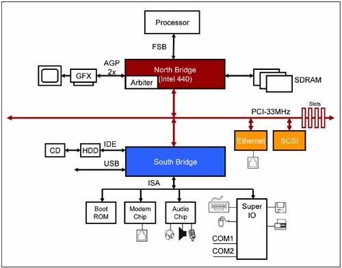
Figure: PCI based system
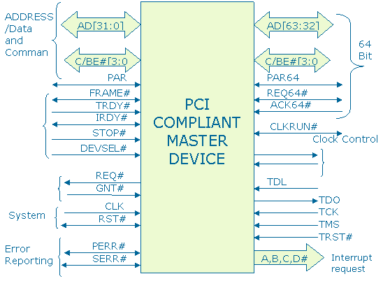
PCI-Compliant master Device Signals
PCI Bus Arbitration
Arbiter
At a given instant in time, one or more PCI bus master devices may require use of the PCI bus to perform a data transfer with another PCI device. Each requesting master asserts its REQ# output to inform the bus arbiter of its pending request for the use of the bus. Figure below illustrates the relationship of the PCI masters to the central PCI resource known as the bus arbiter. In this ezample there are seven possible masters connected to the PCI bus arbiter in the illustration. Each master is connected to the arbiter via a separate pair of REQ# / GNT# signals. Although the arbiter is shown as a separate component, it usually is integrated into the PCI chip set; specifically, it is typically integrated into the host / PCI or the PCI / expansion bus bridge chip.
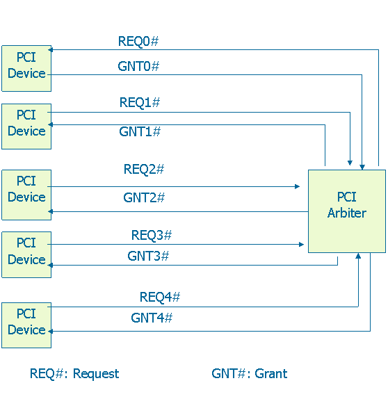
Figure: PCI Arbiter
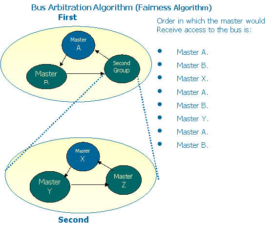
Bus Arbitration algorithm
Summary of Bus Types with Width and Speed
Bus Type |
Bus Width |
Bus Speed |
MB/sec |
ISA |
16 bits |
8 MHz |
16 MBps |
EISA |
32 bits |
8 MHz |
32 MBps |
VL-bus |
32 bits |
25 MHz |
100 MBps |
VL-bus |
32 bits |
33 MHz |
132 MBps |
PCI |
32 bits |
33 MHz |
132 MBps |
PCI |
64 bits |
33 MHz |
264 MBps |
PCI |
64 bits |
66 MHz |
512 MBps |
PCI-X |
64 bits |
133 MHz |
1 GBps |
Although Intel proposed the PCI standard in 1991, it did not achieve popularity until the arrival of Windows 95 (in 1995). This sudden interest in PCI was due to the fact that Windows 95 supported a feature called Plug and Play (PnP).
PCI vs. AGP
The PCI bus was adequate for many years, providing enough bandwidth for all the peripherals most users might want to connect. All except one: graphics cards. In the mid 1990s, graphics cards were getting more and more powerful, and 3D games were demanding higher performance. The PCI bus just couldn't handle all the information passing between the main processor and the graphics processor. As a result, Intel developed the Accelerated Graphics Port (AGP). AGP is a bus dedicated completely to graphics cards. The bandwidth across the AGP bus isn't shared with any other components. Although PCI continues to be the bus of choice for most peripherals, AGP has taken over the specialized task of graphics processing. However, a new bus technology has hit the market that just might spell the end for AGP. More on this later in the article, stay tuned�
Limitations of PCI Architecture
• The maximum frequency achievable with the PCI architecture is 66 MHz. This is a result of the static clock method of driving and latching signals and because reflected-wave signaling is used.
• PCI bus efficiency is in the order of 50% or 60%. Some of the factors that contribute towards this reduced efficiency are listed below.
• The PCI specification allows master and target devices to insert wait-states during data phases of a bus cycle. Slow devices will add wait-states which reduces the efficiency of bus cycles.
• PCI bus cycles do not indicate transfer size. This makes buffer management within master and target devices inefficient.
• Delayed transactions on PCI are handled inefficiently. When a master is retried, it guesses when to try again. If the master tries too soon, the target may retry the transaction again. If the master waits too long to retry, the latency to complete a data transfer is increased. Similarly, if a target disconnects a transaction the master must guess when to resume the bus cycle at a later time.All PCI bus master accesses to system memory result in a snoop access to the CPU cache. Doing so results in additional wait states during PCI bus master accesses of system memory. The North bridge or MCH must assume all system memory address space is cachable even though this may not be the case. PCI bus cycles provide no mechanism by which to indicate an access to non-cachable memory address space.
• PCI architecture observes strict ordering rules as defined by the specification. Even if a PCI application does not require observation of these strict ordering rules, PCI bus cycles do not provide a mechanism to allow relaxed ordering rule. Observing relaxed ordering rules allows bus cycles (especially those that cross a bridge) to complete with reduced latency.
• PCI interrupt handling architecture is inefficient especially because multiple devices share a PCI interrupt signal. Additional software latency is incurred while software discovers which device or devices that share an interrupt signal actually generated the interrupt.
• The processor's NMI interrupt input is asserted when a PCI parity or system error is detected. Ultimately the system shuts down when an error is detected. This is a severe response. A more appropriate response might be to detect the error and attempt error recovery. PCI does not require error recovery features, nor does it support an extensive register set for documenting a variety of detectable errors.
These limitations above have been resolved in the next generation bus architectures, namely PCI-X and PCI Express.
|