Emergence of HDLs
For a long time, programming languages such as FORTRAN , Pascal, and C were being used to describe computer programs that were sequential in nature. Similarly, in the digital design field, designers felt the need for a standard language to describe digital circuits. Thus, Hardware Description Languages (HDLs) came into existence. HDLs allowed the designers to model the concurrency of processes found in hardware elements. Hardware description languages such as Verilog ® HDL and VHDL became popular. Verilog HDL originated in 1983 at Gateway Design Automation. Later, VHDL was developed under contract from DARPA. Using both Verilog and VHDL simulators to simulate large digital circuits quickly gained acceptance from designers. Even though HDLs were popular for logic verification, designers had to manually translate the HDL-based design into a schematic circuit with interconnections between gates. The advent of logic synthesis in the late 1980s changed the design methodology radically. Digital circuits could be described at a register transfer level (RTL) by use of an HDL. Thus, the designer had to specify how the data flows between registers and how the design processes the data. The details of gates and their interconnections to implement the circuit were automatically extracted by logic synthesis tools from the RTL description. Thus, logic synthesis pushed the HDLs into the forefront of digital design. Designers no longer had to manually place gates to build digital circuits. They could describe complex circuits at an abstract level in terms of functionality and data flow by designing those circuits in HDLs. Logic synthesis tools would implement the specified functionality in terms of gates and gate interconnections. HDLs also began to be used for system-level design. HDLs were used for simulation of system boards, interconnect buses, FPGAs (Field Programmable Gate Arrays), and PALs (Programmable Array Logic). A common approach is to design each IC chip, using an HDL, and then verify system functionality via simulation. Today, Verilog HDL is an accepted IEEE standard. In 1995, the original standard IEEE 1364-1995 was approved. IEEE 1364-2001 is the latest Verilog HDL standard that made significant improvements to the original standard.
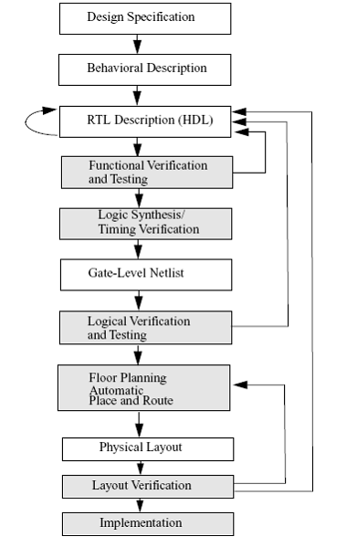
Typical Design Flow
A typical design flow for designing VLSI IC circuits is shown in Figure.
Unshaded blocks show the level of design representation; shaded blocks show processes in the design flow.
Importance of HDLs
HDLs have many advantages compared to traditional schematic-based design.
� Designs can be described at a very abstract level by use of HDLs. Designers can write their RTL description without choosing a specific fabrication technology. Logic synthesis tools can automatically convert the design to any fabrication technology. If a new technology emerges, designers do not need to redesign their circuit. They simply input the RTL description to the logic synthesis tool and create a new gate-level netlist, using the new fabrication technology. The logic synthesis tool will optimize the circuit in area and timing for the new technology.
� By describing designs in HDLs, functional verification of the design can be done early in the design cycle. Since designers work at the RTL level, they can optimize and modify the RTL description until it meets the desired functionality. Most design bugs are eliminated at this point. This cuts down design cycle time significantly because the probability of hitting a functional bug at a later time in the gate-level netlist or physical layout is minimized.
� Designing with HDLs is analogous to computer programming. A textual description with comments is an easier way to develop and debug circuits. This also provides a concise representation of the design, compared to gate-level schematics. Gate-level schematics are almost incomprehensible for very complex designs.
HDL-based design is here to stay.With rapidly increasing complexities of digital circuits and increasingly sophisticated EDA tools, HDLs are now the dominant method for large digital designs. No digital circuit designer can afford to ignore HDL-based design.
Popularity of Verilog HDL
Verilog HDL has evolved as a standard hardware description language. Verilog HDLoffers many useful features for hardware design.
� Verilog HDL is a general-purpose hardware description language that is easy to learn and easy to use. It is similar in syntax to the C programming language. Designers with C programming experience will find it easy to learn Verilog HDL.
� Verilog HDL allows different levels of abstraction to be mixed in the same model. Thus, a designer can define a hardware model in terms of switches, gates, RTL, or behavioral code. Also, a designer needs to learn only one language for stimulus and hierarchical design.
� Most popular logic synthesis tools support Verilog HDL. This makes it the language of choice for designers.
�All fabrication vendors provide Verilog HDL libraries for postlogic synthesis simulation. Thus, designing a chip in Verilog HDL allows the widest choice of vendors.
� The Programming Language Interface (PLI) is a powerful feature that allows the user to write custom C code to interact with the internal data structures of Verilog. Designers can customize a Verilog HDL simulator to their needs with the PLI.
Program Structure
Verilog programs are composed of a set of modules . Each module can be thought of as a function in C � it's a set of lower-level routines which can be reused in your main program.
Thus, the Verilog programming model resembles one of an imperative programming language like C: the main program, composed of functions (each of which takes inputs as parameters and returns output values), itself takes inputs and returns outputs, mapped to some pins in your digital system. Below is an example of what a very simple Verilog program looks like
// A simple Verilog program that implements a not-too-complicated logic
// function of four variables: (A NAND B) NAND (C NAND D)
module mynand(in1, in2, out);
input in1, in2;
output out;
assign out = ~(in1 & in2);
endmodule
// This is the main program
module somefunction(p, q, p_b, q_b, o);
input p, q, p_b, q_b;
output o;
wire w, w_b;
mynand nand1(p, q, w);
mynand nand2(p_b, q_b, w_b);
mynand nand3(w, w_b, o);
endmodule
Let's analyze this program: first, it consists of a low-level module that implements a nand gate (called mynand ) and the main program somefunction which uses three mynand modules. mynand takes three arguments: two of them are inputs and the third is the output, which is specified in the header of the module. The output wire is assigned a value � the logical NAND of in1 and in2 .
somefunction Takes four inputs and one output. It uses intermediate values w and w b to wire up two NAND gates together with another NAND gate.
One important thing that you, a beginning Verilog user, need to consider is that module in- vocation and assignments are not imperative in nature. We are not really assigning anything to the variable called out . Similarly, w and w b are not local variables. Instead, you should think of the statement assign as something that wires up the right-hand side with the left- hand side, and think of all inputs, outputs and intermediate values are physical wires. So all that mynand does is take in1 and in2 (whatever wires they may end up being), wire them up with an NAND and wire the output to out . So, calling nand1(p, q, w) simply wires up p and q in an NAND whose output becomes w . This visual representation (inputs and outputs as wires) will help you avoid many mistakes when coding your system in Verilog. Sometimes (if you're using a foreign module for which you only have signal names) you may need to use the extended Verilog module calling syntax, which lets you rearrange the order of signals passed to the module. For example, you could replace mynand nand1(p, q, w) with the following:
mynand nand1(.out(w), .in1(p), .in2(q))
Syntax Basics
Assign causes the left-hand side to be updated any time the right hand side changes. This is equivalent to saying that it wires up the left hand side with the right hand side. Assign causes a permanent link between the two, in a sense that it makes no sense to reassign the same inputs and outputs. _ a negates the input a . a & b ANDs the two inputs together, a | b ORs them together, while ^ performs a logical XOR on a and b . Hence, _ (a | b) implements a NOR function.
Verilog uses C-style comments. // marks the beginning of a line of comments. Moreover, anything between /* and */ is also treated as a comment.
Verilog supports the C ternary operator, as in assign y = s ? d1 : d0;
assigns y to d1 if s is 1 and to d0 otherwise. The ternary operator implements the simplest 2:1 multiplexer (you will learn about these later on in class).
Verilog also supports ordinary C operators like + , - , * , < , > , < =, > =, ==, ! =, << , >> , / and % . A work of caution, though, is that some of these operators are really expensive in hardware. To implement a multiplier, a large number of gates need to be used, so when possible avoid using these. In particular, in class we will ask you to never use any of these operators unless specifically told to do so.
Operator precedence follows the rules present in the C syntax. The following table shows all the operators and their precedence, from highest to lowest
_
* , / , %
+ , -
<< , >>
< , < =, > , > =
=, ==, ! =
& , _ &
^ , _ ^
| , _ |
?:
Constants may be specified in many bases, though we will stick to binary and hexadecimal. To represent a number in binary, specify the length of the number in bits (though optional, this is highly recommended), followed by an apostrophe, followed by the sequence of zeroes and ones (leading zeroes may be omitted. For example, the number 5 can be specified as 8'b101 Hexadecimal numbers have an additional h after the apostrophe. A number 139 can be specified as 8'h8B Omitted bases are treated as decimal numbers, but these will be stored with a number of leading zeroes, which leads to inefficient design. It is advantageous to use specified bases. A special value, High-Z, can be used, and is denoted as a binary z , e.g. 4'bz You will learn more about High-Z values later on in the course. You can define constants with parameter , for example:
parameter SEVEN = 4'b0111;
Finally, if you want to explicitly specify a delay of a statements, you can do it by following the keyword with a pound-number, as in the following example:
assign #42 y = _ a
Buses You will notice soon that one-bit signals are simply not enough. Instead of tediously defining hundreds of input and output wires and wiring them separately, Verilog supports buses, i.e. collections of wires on which similar functions are performed. To define a bus, specify the highest and the lowest bit of a bus in square brackets next to the signal's name.
For example,
module inv(a, y);
input [3:0] a;
output [3:0] y;
assign y = ~a;
endmodule
defines two four-wire buses (remember that we count from zero!) and assigns y to be a NOT of a , i.e. each wire in y is hooked up to a corresponding wire in a by a NOT gate. Note that all bitwise operations (described in the previous section) work on buses, too. Sometimes a need may emerge to collapse, or reduce a bus to a single wire with some function. Reduction operators let you take all wires of a bus, connect them to a single multi-input function, and assign the output to a single wire. These operators are & , | , ^ , _ & and _ | , placed in front of the bus, for AND, OR, XOR, NAND and NOR respectively.
For example,
module and8(a, y);
input [7:0] a;
output y;
assign y = &a;
endmodule;
implements an 8-input, 1-output AND gate. Note that a multi-input XOR is a parity function, returning 1 if an odd number of inputs are 1. It is also possible to take subsets of wires from buses. This is achieved by specifying the high and the low wire used in square brackets. For example, if a and b are 8-bit buses, the following is used to AND the high four bits of a and the low four bits of b : and4(a[7:4], b[3:0]) Moreover, it is possible to combine buses. This is achieved by grouping buses (or subsets of buses) in curly braces, prefixing repeated components with a number. Grouped buses may appear on the left-hand side, as well as the right-hand side of an expression. For example, to create a 16-bit bus composed of three copies of a 4-bit bus, two upper bits of another 4-bit bus, and two zeroes as the least significant bits, we would write
input [3:0] a, b;
output [15:0] y;
assign y = {3{a[3:0]}, b[3:2], 2'b00}
Do you see why specifying lengths of binary constants is a good idea?
5 Combining Values
All Verilog signals have one of four values at a time. These values are:
� 0 � Low (false)
� 1 � High (true)
� X � Undefined
� Z � High-Z (floating, high impedance)
You will learn about a High-Z value later on in the course. For now it should suffice to say that a High-Z is something like an �unimportant� value, so if two wires are combined, High-Z always gives way to the other value. The table below explains what happens if you combine values:
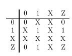
So combining a 0 and a High-Z, for instance, results in a 0. Let's show an example of tristate
(0, 1, and High-Z) logic:
module tristate(a, en, y);
input [3:0] a;
input en;
output [3:0] y;
assign y = en ? a : 4'bz;
endmodule
module mux2(d0, d1, s, y);
input [3:0] d0, d1;
input s;
output [3:0] y;
tristate t0(d0, ~s, y);
tristate t1(d1, s, y);
endmodule
Let's see what exactly is going on here. First a tristate buffer module is defined. This buffer will simply carry its input over if enable en is 1, or output High-Z otherwise. Then, a mux2 module wires up two such buffer in a way that exactly one is High-Z and the other one is either 0 or 1. Notice that both tristate buffers have been wired to the same output � y . This is allowed since High-Z is combined with a 0 or a 1 here. More Complex Language Constructs always is a statement that lets you define blocks of code, in which assignments will only happen as selected signals (specified in the header of the statement) change.
For example,
input a, d
reg out
always @(a or d)
out = d
sets out to d only if the value of a or the value of d changes. Notice a slightly different syntax (we're using the word or as opposed to the symbol | , and = instead of assign ). Another possibility is to specify that an assignment happens on the rising (or falling) clock edge. If clk is the clock input,
always @(posedge clk)
achieves this task. Notice that all signals on the left-hand side of the = sign inside always blocks must be declared as reg , not wire . All such signals will be initialized to X (see section on four values in Verilog).
If you need to perform more than one operation under the always block, you need to enclose the operations with begin and end . always is most often combined with if (and possibly else if and else ) to create powerful sequential logic systems. Study the following example:
always begin
if (a==2'b01) b = 2'b01;
else if (a>2'b01) begin
b = a;
c = 1;
end
end
Two possible assignment syntaxes are a = b and a <= b . The difference lies in concurrency � all expressions of the former type are evaluated sequentially while all expressions of the latter type are evaluated in parallel. For example,
a <= b
b <= a
swaps the values of a and b while
a = b
b = a
simply sets both a and b to the previous value of b (the second assignment is using the value of a from the first assignment). Concurrent assignment can get really confusing and so it is recommended that you use the sequential = . One very useful construct, which only works in the always block, is case . The following example shows how to construct a decoder (a logic device which takes a k -wire wide bus which carries a binary number l (0 6 l 6 2 k - 1), and outputs a 2 k -wire wide bus such that the only wire that's set to 1 is wire l :
module my_decoder(a, y);
input [2:0] a;
output [7:0] y;
reg [7:0] y;
always @(a)
case (a)
3'b000: y = 8'b00000001;
3'b001: y = 8'b00000010;
3'b010: y = 8'b00000100;
3'b011: y = 8'b00001000;
3'b100: y = 8'b00010000;
3'b101: y = 8'b00100000;
3'b110: y = 8'b01000000;
3'b111: y = 8'b10000000;
endcase
endmodule
The expression inside of case may also be a concatenated bus, for example
case ( { a, b } ) will help you draw out a truth table for a two-input logic.
casez is a variation of case which allows the use of Don't-cares in the constants being evaluated. For instance, the following is acceptable:
casez (a)
3'b0??: y = 1'b0;
3'b101: y = 1'b0;
3'b100: y = 1'b1;
3'b11?: y = 1'b1;
Endcase
7 Common errors
Below is a brief list of common errors that you may commit writing modules in Verilog:
� You are using sequential logic outside of the always block, or unnecessarily using
combinational logic in the always block (unless case is necessary)
� You are getting Verilog's X values. Make sure all outputs are defined, you don't short- circuit outputs (wire outputs to more than one module without a High-Z) and that your if - else logic works correctly (you're not skipping any cases)
� You are missing begin - end block in your always statement