Animated PCI Express
Introduction
PCI Express is the third generation high performance I/O bus used to interconnect peripheral devices in applications such as computing and communication platforms. The first generation buses include the ISA, EISA, VESA, and Micro Channel buses, while the second generation buses include PCI, AGP, and PCI-X. PCI Express is an all encompassing I/O device interconnects bus that has applications in the mobile, desktop, workstation, server, embedded computing and communication platforms.
The PCI bus has served us well for the last 10 years and it will play a major role in the next few years. However, today's and tomorrow's processors and I/O devices are demanding much higher I/O bandwidth than PCI 2.2 or PCI-X can deliver and it is time to engineer a new generation of PCI to serve as a standard I/O bus for future generation platforms. There have been several efforts to create higher bandwidth buses and this has resulted in the PC platform supporting a variety of application-specific buses alongside the PCI I/O expansion bus. As shown in the figure 1:
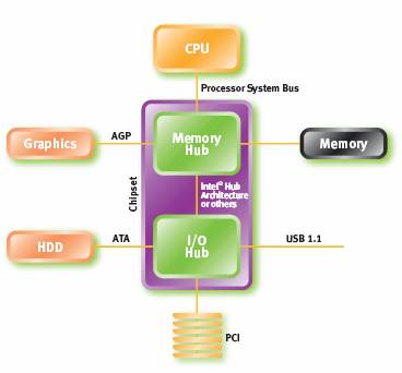
Figure: 1
The processor system bus continues to scale in both frequency and voltage at a rate that will continue for the foreseeable future. Memory bandwidths have increased to keep pace with the processor. Indeed, as shown in figure1, the chipset is typically partitioned as a memory hub and an I/O hub since the memory bus often changes with each processor generation.
One of the major functions of the chipset is to isolate these ever-changing buses from the stable I/O bus. Close Investigation of the 1990's PCI signaling technology reveals a multi-drop, parallel bus implementation that is close to its practical limit of performance: it cannot be easily scaled up in frequency or down in voltage; its synchronously clocked data transfer is signal skew limited and the signal routing rules are at the limit for cost-effective FR4 technology. All approaches to pushing these limits to create a higher bandwidth, general-purpose I/O bus result in large cost increases for little performance gain. The desktop solution of figure: 1 is only part of the problem of diverging local I/O bus standards. To PCI's credit it has been used in applications not envisaged by the original specification writers and variants and extensions of PCI can be found in desktop, mobile, server and embedded communications market segments.
What makes up the PCI-Express bus?
The PCI-Express bus is composed of multiple lanes of point-to-point wired copper interconnects serving all the components that used to just drop data into the older PCI bus. To make things even more flexible, a switch has been added to the architecture.
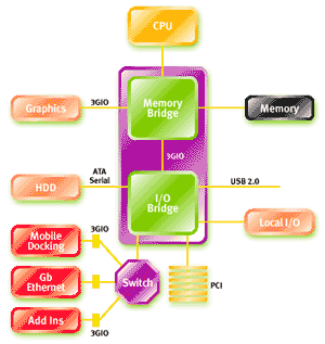
Figure: 2
Working in principle just like an Ethernet switch, this is intended to sit between the PCI-Express devices connected to the board and the rest of the I/O system. This will enable newer devices, for example PCI-Express connected on board Gigabit controllers or 10/100 gigabit network cards, to communicate with each other directly if necessary. By adding in this shortcut the data need not go through the chipset to reach an adjacent device.
Compatibility between PCI 2.2 and PCI-Express
The PCI-Express bus will be completely software compatible with PCI 2.2 compliant devices. Intel has already stated that all current operating systems will support PCI 2.2 compatible interface cards in the new PCI-Express system using the existing PCI drivers.
This is an essential requirement if PCI-Express technology is to gain widespread acceptance. Forced obsolescence does not tend to go over well with computer users.
The current specifics allow for an additional header placed at the end of a standard PCI slot to support lower bandwidth (1-2 lane) PCI-Express devices, somewhat similar to the extra connector used for 66mhz PCI devices.
Understanding PCI Express Fundamentals
PCI Express provides a high-speed, high-performance, point-to-point, dual simplex, differential signaling Link for interconnecting devices. Data is transmitted from a device on one set of signals, and received on another set of signals.
The Link - A Point-to-Point Interconnect
As shown in Figure 3, a PCI Express interconnect consists of either a x1, x2, x4, x8, x12, x16 or x32 point-to-point Link. A PCI Express Link is the physical connection between two devices. A Lane consists of signal pairs in each direction. A x1 Link consists of 1 Lane or 1 differential signal pair in each direction for a total of 4 signals. A x32 Link consists of 32 Lanes or 32 signal pairs for each direction for a total of 128 signals. The Link supports a symmetric number of Lanes in each direction. During hardware initialization, the Link is initialized for Link width and frequency of operation automatically by the devices on opposite ends of the Link. No OS or firmware is involved during Link level initialization.
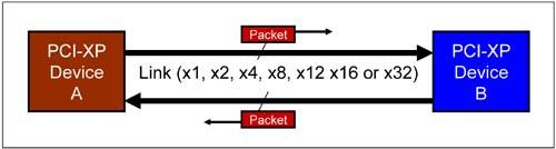
Figure 3. PCI Express Link
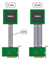
Figure: 4 Links and Lanes
Differential Signaling
PCI Express devices employ differential drivers and receivers at each port. Figure 5 shows the electrical characteristics of a PCI Express signal. A positive voltage difference between the D+ and D- terminals implies Logical 1. A negative voltage difference between D+ and D- implies a Logical 0. No voltage difference between D+ and D- means that the driver is in the high-impedance tristate condition, which is referred to as the electrical-idle and low-power state of the Link.

Figure 5. PCI Express Differential Signal
The PCI Express Differential Peak-to-Peak signal voltage at the transmitter ranges from 800 mV - 1200 mV, while the differential peak voltage is one-half these values. The common mode voltage can be any voltage between 0 V and 3.6 V. The differential driver is DC isolated from the differential receiver at the opposite end of the Link by placing a capacitor at the driver side of the Link. Two devices at opposite ends of a Link may support different DC common mode voltages. The differential impedance at the receiver is matched with the board impedance to prevent reflections from occurring.
Switch
PCIe's most drastic and obvious improvement over PCI is its point-to-point bus topology. Take a look at the following diagram, and compare it to the layout of the PCI bus.
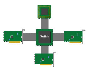
Figure: 6 The Shared Switch
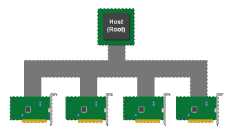
Figure: 7 The Shared Bus
In a point-to-point bus topology, a shared switch replaces the shared bus as the single shared resource by means of which all of the devices communicate. Unlike in a shared bus topology, where the devices must collectively arbitrate among themselves for use of the bus, each device in the system has direct and exclusive access to the switch. In other words, each device sits on its own dedicated bus, which in PCIe lingo is called a link .
Like a router in a network or a telephone switchbox, the switch routes bus traffic and establishes point-to-point connections between any two communicating devices on a system. To return to our office analogy from the previous section, each employee has his or her own private line to the front desk; so instead of shouting over a shared line to get a particular employee's attention, the front desk secretary uses a switchboard to connect employees directly to incoming callers and to each other.
In the point-to-point diagram above, the CPU at the top can talk to any of the PCIe devices by "dialing" that device's address and opening up a direct and private communications link, via the switch, with it. Of course, as with a modern telephone call, or even better, an internet connection between a browser and a website, the two communicating parties only think they're talking to each other via a private, direct, continuous link; in reality, though, the communications stream is broken up into discrete packets of data, which the switch routes � like a postal worker delivering addressed envelopes � back and forth between the two parties.
Rootcomplex
The Root Complex denotes the device that connects the CPU and memory subsystem to the PCI Express fabric. It may support one or more PCI Express ports. The root complex in this example supports 3 ports. Each port is connected to an endpoint device or a switch which forms a sub-hierarchy. The root complex generates transaction requests on the behalf of the CPU. It is capable of initiating configuration transaction requests on the behalf of the CPU. It generates both memory and IO requests as well as generates locked transaction requests on the behalf of the CPU. The root complex as a completer does not respond to locked requests. Root complex transmits packets out of its ports and receives packets on its ports which it forwards to memory. A multi-port root complex may also route packets from one port to another port but is NOT required by the specification to do so.
Root complex implements central resources such as: hot plug controller, power management controller, interrupt controller, error detection and reporting logic. The root complex initializes with a bus number, device number and function number which are used to form a requester ID or completer ID. The root complex bus, device and function numbers initialize to all 0s.
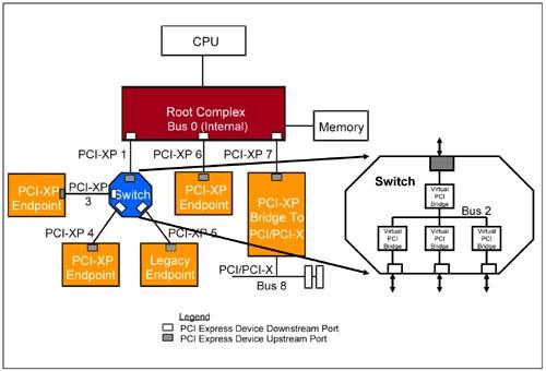
Figure 8
Endpoints
Endpoints are devices other than root complex and switches that are requesters or completers of PCI Express transactions. They are peripheral devices such as Ethernet, USB or graphics devices. Endpoints initiate transactions as a requester or respond to transactions as a completer. Two types of endpoints exist, PCI Express endpoints and legacy endpoints. Legacy Endpoints may support IO transactions. Each endpoint is initialized with a device ID ( requester ID or completer ID) which consists of a bus number, device number, and function number. Endpoints are always device 0 on a bus.
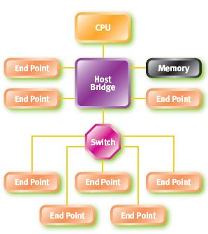
Figure: 9 Switch added to PCI-Express topology
Multi-Function Endpoints
Like PCI devices, PCI Express devices may support up to 8 functions per endpoint with at least one function number 0. However, a PCI Express Link supports only one endpoint numbered device 0.
Requester
A Requester is a device that originates a transaction in the PCI Express fabric. Root complex and endpoints are requester type devices.
Completer
A Completer is a device addressed or targeted by a requester. A requester reads data from a completer or writes data to a completer. Root complex and endpoints are completer type devices.
Port
A Port is the interface between a PCI Express component and the Link. It consists of differential transmitters and receivers. An Upstream Port is a port that points in the direction of the root complex. A Downstream Port is a port that points away from the root complex. An endpoint port is an upstream port. A root complex port(s) is a downstream port. An Ingress Port is a port that receives a packet. An Egress Port is a port that transmits a packet.
PCI-Express System
The following diagram shows the typical PCI-Express System.
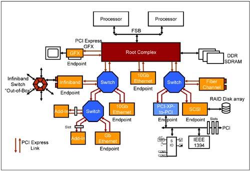
Figure 10
PCI �Express Architecture
Packet Based Protocol
Rather than bus cycles we are familiar with from PCI and PCI-X architectures, PCI Express encodes transactions using a packet based protocol. Packets are transmitted and received serially and byte striped across the available Lanes of the Link. The more Lanes implemented on a Link the faster a packet is transmitted and the greater the bandwidth of the Link. The packets are used to support the split transaction protocol for non-posted transactions. Various types of packets such as memory read and write requests, IO read and write requests, configuration read and write requests, message requests and completions are defined.
PCI-Express Requester/Completer Split Transaction Model
Consider an example of the split transaction protocol supported by PCI-Express for delaying transactions. This protocol is illustrated in Figure 11 . A requester initiates a read transaction. The completer that claims the bus cycles may be unable to return the requested data immediately. Rather than signaling a retry as would be the case in PCI protocol, the completer memorizes the transaction (address, transaction type, byte count, requester ID are memorized) and signals a split response. This prompts the requester to end the bus cycle, and the bus goes idle. The PCI-Express bus is now available for other transactions, resulting in more efficient bus utilization. Meanwhile, the requester simply waits for the completer to supply it the requested data at a later time. Once the completer has gathered the requested data, it then arbitrates and obtains bus ownership and initiates a split completion bus cycle during which it returns the requested data. The requester claims the split completion bus cycle and accepts the data from the completer.
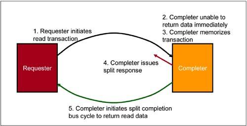
Figure 11. PCI-Express Split Transaction Protocol
The split completion bus cycle is very much like a write bus cycle. Exactly two bus transactions are needed to complete the entire data transfer. In between these two bus transactions (the read request and the split completion transaction) the bus is utilized for other transactions. The requester also receives the requested data in a very efficient manner.
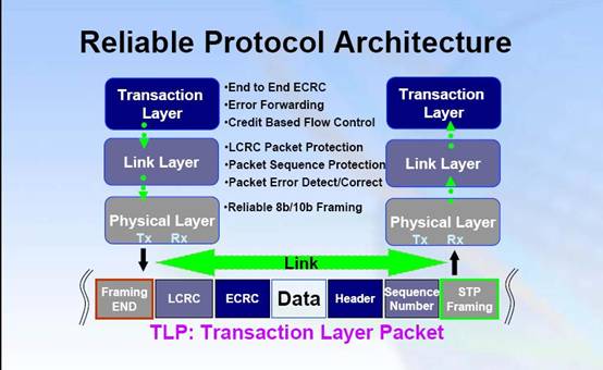
Figure 12: Reliable Protocol Architecture for PCI-Express
The PCI Express Architecture is specified in layers as shown in Figure 13. Compatibility with the PCI addressing model (a load-store architecture with a flat address space) is maintained to ensure that all existing applications and drivers operate unchanged. PCI Express configuration uses standard mechanisms as defined in the PCI Plug-and-Play specification. The software layers will generate read and write requests that are transported by the transaction layer to the I/O devices using a packet-based, split-transaction protocol. The link layer adds sequence numbers and CRC to these packets to create a highly reliable data transfer mechanism. The basic physical layer consists of a dual-simplex channel that is implemented as a transmit pair and a receive pair. The initial speed of 2.5 Giga transfers/second/direction provides a 200MB/s communications channel that is close to twice the classic PCI data rate.
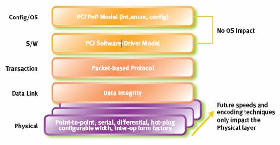
Figure 13. The PCI Express Architecture is specified in layers
Physical Layer
The fundamental PCI Express link consists of two, low-voltage, differentially driven pairs of signals: a transmit pair and a receive pair as shown in Figure 14. A data clock is embedded using the 8b/10b encoding scheme to achieve very high data rates. The initial frequency is 2.5 Giga transfers/second/direction and this is possible to increase with silicon technology advances of up to 10 Giga transfers/second/direction (the theoretical maximum for signals in copper). The physical layer transports packets between the link layers of two PCI Express agents.
The bandwidth of a PCI Express link may be linearly scaled by adding signal pairs to form multiple lanes. The physical layer supports x1, x2, x4, x8, x12, x16 and x32 lane widths and splits the byte data as shown in Figure 9. Each byte is transmitted, with 8b/10b encoding, across the lane(s). This data disassembly and re-assembly is transparent to other layers.
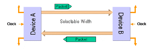
Figure 14 A PCI Express link uses transmit and receive signal pairs
The bandwidth of a PCI Express link may be linearly scaled by adding signal pairs to form multiple lanes. The physical layer supports x1, x2, x4, x8, x12, x16 and x32 lane widths and splits the byte data as shown in Figure 15. Each byte is transmitted, with 8b/10b encoding, across the lane(s). This data disassembly and re-assembly is transparent to other layers.
During initialization, each PCI Express link is set up following a negotiation of lane widths and frequency of operation by the two agents at each end of the link. No firmware or operating system software is involved.
The PCI Express architecture comprehends future performance enhancements via speed upgrades and advanced encoding techniques. The future speeds, encoding techniques or media would only impact the physical layer.
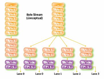
Figure 15. A PCI Express Link consists of one or more lanes
Link Layer
The primary role of a link layer is to ensure reliable delivery of the packet across the PCI Express link. The link layer is responsible for data integrity and adds a sequence number and a CRC to the transaction layer packet as shown in Figure 16.
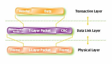
Figure 16. The Link Layer adds data integrity features
Most packets are initiated at the Transaction Layer (next section). A credit-based, flow control protocol ensures that packets are only transmitted when it is known that a buffer is available to receive this packet at the other end. This eliminates any packet retries, and their associated waste of bus bandwidth due to resource constraints. The Link Layer will automatically retry a packet that was signaled as corrupted.
Transaction Layer
The transaction layer receives read and write requests from the software layer and creates request packets for transmission to the link layer. All requests are implemented as split transactions and some of the request packets will need a response packet. The transaction layer also receives response packets from the link layer and matches these with the original software requests. Each packet has a unique identifier that enables response packets to be directed to the correct originator. The packet format supports 32bit memory addressing and extended 64bit memory addressing. Packets also have attributes such as �no-snoop�, �relaxed-ordering� and �priority� which may be used to optimally route these packets through the I/O subsystem.
The transaction layer supports four address spaces: it includes the three PCI address spaces (memory, I/O and configuration) and adds a Message Space. PCI 2.2 introduced an alternate method of propagating system interrupts called Message Signaled Interrupt (MSI). Here a special-format memory write transaction was used instead of a hard-wired sideband signal. This was an optional capability in a PCI 2.2 system. The PCI Express specification re-uses the MSI concept as a primary method for interrupt processing and uses Message Space to support all prior side-band signals, such as interrupts, power-management requests, resets, and so on, as in-band Messages. Other �special cycles� within the PCI 2.2 specification, such as Interrupt Acknowledge, are also implemented as in-band Messages. You could think of PCI Express Messages as �virtual wires� since their effect is to eliminate the wide array of sideband signals currently used in a platform implementation.
Software Layers
Software compatibility is of paramount importance for a third generation local I/O bus. There are two facets of software compatibility; initialization, or enumeration, and run-time. PCI has a robust initialization model wherein the operating system can discover all of the add-in hardware devices present and then allocate system resources, such as memory, I/O space and interrupts, to create an optimal system environment. The PCI configuration space and the programmability of I/O devices are key concepts that are unchanged within the PCI Express Architecture; in fact, all operating systems will be able to boot without modification on a PCI Express-based platform.
The run-time software model supported by PCI is a load-store, shared memory model � this is maintained within the PCI Express Architecture which will enable all existing software to execute unchanged. New software may use new capabilities.